

HIT HD74HC4538 Datasheet
HD74HC4538
Dual Precision Retriggerable/Resettable Monostable
Multivibrators
Description
Each multivibrator features both a negative, A, and a positive, B, transition triggered input, either of which
can be used as an inhibit input. Also included is a clear input that when taken low resets the one short. The
HD74HC4538 is retriggerable. That is, it may be triggered repeatedly while their outputs are generating a
pulse and the pulse will be extended.
Pulse width stability over a wide range of temperature. The output pulse equation is simply: tw = 0.7 (R)
(C).
Features
• High Speed Operation: tpd (A or B to Y) = 22 ns typ (CL = 50 pF)
• High Output Current: Fanout of 10 LSTTL Loads
• Wide Operating Voltage: VCC = 2 to 6 V
• Low Input Current: 1 µA max
• Low Quiescent Supply Current
Function Table
Inputs Outputs
C
D
LXXLH
HL
H H
HH Not triggered
H L Not triggered
X : Irrelevant
ABQQ
HD74HC4538
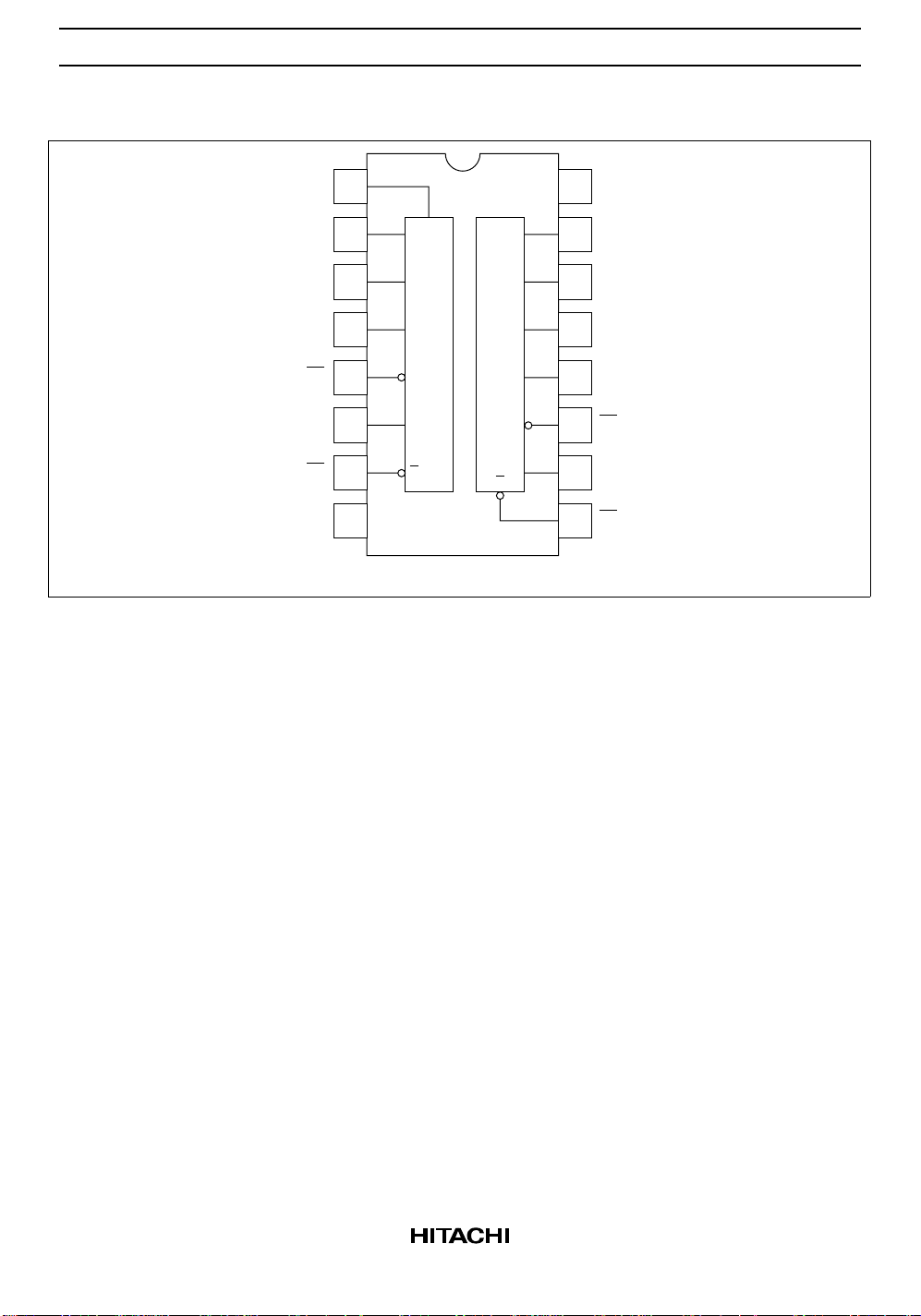
Pin Arrangement
T
1A
T
2A
CD
A
B
Q
Q
GND
1
T
2
3
A
4
A
5
A
6
A
7
A
T
CD
A
B
Q
Q
1
2
T
T
CD
Q
8
16
V
CC
15
14
13
12
11
10
T
1B
T
2B
CD
B
A
B
B
B
Q
B
9
Q
B
1
2
A
B
Q
(Top view)
2

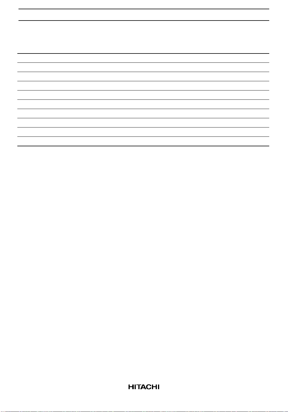
Block Diagram
HD74HC4538
C
X
T
1A
A
A
B
A
C
A
B
DA
T
1B
B
B
C
X
R
X
V
CC
T
2A
Q
A
Q
A
R
X
V
CC
T
2B
Q
B
Q
B
C
DB
RX and CX are external components
3
HD74HC4538
Absolute Maximum Ratings
Item Symbol Rating Unit
Supply voltage range V
CC
Input voltage Vin –0.5 to VCC + 0.5 V
Output voltage Vout –0.5 to VCC + 0.5 V
DC input diode current I
DC input diode current pin 2, 14 I
DC output diode current I
IK
IK
OK
DC current drain per pin Iout ±25 mA
DC current drain per VCC, GND ICC, I
Power dissipation per package P
GND
T
Storage temperature Tstg –65 to +150 °C
–0.5 to +7.0 V
±20 mA
±30 mA
±20 mA
±50 mA
500 mW
4
HD74HC4538
DC Characteristics
Ta = –40 to
Ta = 25°C
Item Symbol V
Input voltage V
IH
(V) Min Typ Max Min Max Unit Test Conditions
CC
2.0 1.5 — — 1.5 — V
4.5 3.15 — — 3.15 —
6.0 4.2 — — 4.2 —
V
IL
2.0 — — 0.5 — 0.5 V
4.5 — — 1.35 — 1.35
6.0 — — 1.8 — 1.8
Output voltage V
OH
2.0 1.9 2.0 — 1.9 — V Vin = VIH or VILIOH = –20 µA
4.5 4.4 4.5 — 4.4 —
6.0 5.9 6.0 — 5.9 —
4.5 4.18 — — 4.13 — IOH = –4 mA
6.0 5.68 — — 5.63 — IOH = –5.2 mA
V
OL
2.0 — 0.0 0.1 — 0.1 V Vin = VIH or VILIOL = 20 µA
4.5 — 0.0 0.1 — 0.1
6.0 — 0.0 0.1 — 0.1
4.5 — — 0.26 — 0.33 IOL = 4 mA
6.0 — — 0.26 — 0.33 IOL = 5.2 mA
Input current Iin 6.0 — — ±0.1 — ±1.0 µA Vin = VCC or GND
Quiescent supply
I
CC
6.0 — — 130 — 220 µA Vin = VCC or GND,
current
(standby state)
Current drain
I
CC
6.0 — — 130 — 220 µA Vin = VCC or GND,
(active state)
+85°C
Q
= QB = GND, Iout = 0 µA
A
Q
= QB = V
A
CC
Pin 2, 14 = 0.5 V
CC
5
 Loading...