HIT HD74HC444, HD74HC443, HD74HC442 Datasheet

HD74HC442/HD74HC443/HC74HC444
Quad. Tridirectional Bus Transceiver
(with noninverted 3-state outputs)
Quad. Tridirectional Bus Transceiver
(with inverted 3-state outputs)
Quad Tridirectional Bus Transceiver
(with noninverted/inverted 3-state outputs)
Description
These bus transceivers are designed for a synchronous three-way communication between four-line data
buses. They give the designer a choice of selecting inverting, noninverting or a combination of inverting
and noninverting data paths with 3-state outputs.
The S0 and S1 inputs select the bus from which data are to be transferred. The G inputs enable the bus or
buses to which data are to be transferred. The port for any bus selected for input and any other bus not
enabled for output will be at high impedance.
Features
• High Speed Operation
• High Output Current: Fanout of 15 LSTTL Loads
• Wide Operating Voltage: VCC = 2 to 6 V
• Low Input Current: 1 µA max
• Low Quiescent Supply Current: ICC (static) = 4 µA max (Ta = 25°C)

HD74HC442/HD74HC443HD74HC444
Function Table
Inputs Transfers Between Buses
S
CS S
H X X X X X None None None
X H H X X X None None None
X X X H H H None None None
X L L X H H None None None
X L H H X H None None None
X H L H H X None None None
LLLXLLA → B, A → C A → B, A → C A → B, A → C
L LHLXLB → C, B → A B → C, B → AB → C, B → A
L HLLLXC → A, C → B C → A, C → B C → A, C → B
LLLXLHA → B A → B A → B
L LHHXLB → C B → CB → C
L HLLHXC → A C → A C → A
LLLXHLA → C A → C A → C
L LHLXHB → A B → A B → A
LHLHLXC → B C → BC → B
1
GA GB GC HD74HC442 HD74HC443 HD74HC444
0
2

Pin Arrangement
(
)
HD74HC442/HD74HC443/HD74HC444
GND
Absolute Maximum Ratings
1
2
1
B
C1
3
4
C2
B2
5
B3
6
C3
7
C4
8
B4
9
10 11
Top view
20CS
19
18
17
16
15
14
13
12
V
GC
GB
GA
A1
A2
A3
A4
S1
S0
CC
Item Symbol Rating Unit
Supply voltage range V
Input voltage V
Output voltage V
Output current I
CC
IN
OUT
OUT
DC current drain per VCC GND ICC, I
DC input diode current I
DC output diode current I
Power Dissipation per package P
IK
OK
T
GND
–0.5 to +7.0 V
–0.5 to VCC + 0.5 V
–0.5 to VCC + 0.5 V
±35 mA
±75 mA
±20 mA
±20 mA
500 mW
Storage temperature Tstg –65 to +150 °C
3

HD74HC442/HD74HC443HD74HC444
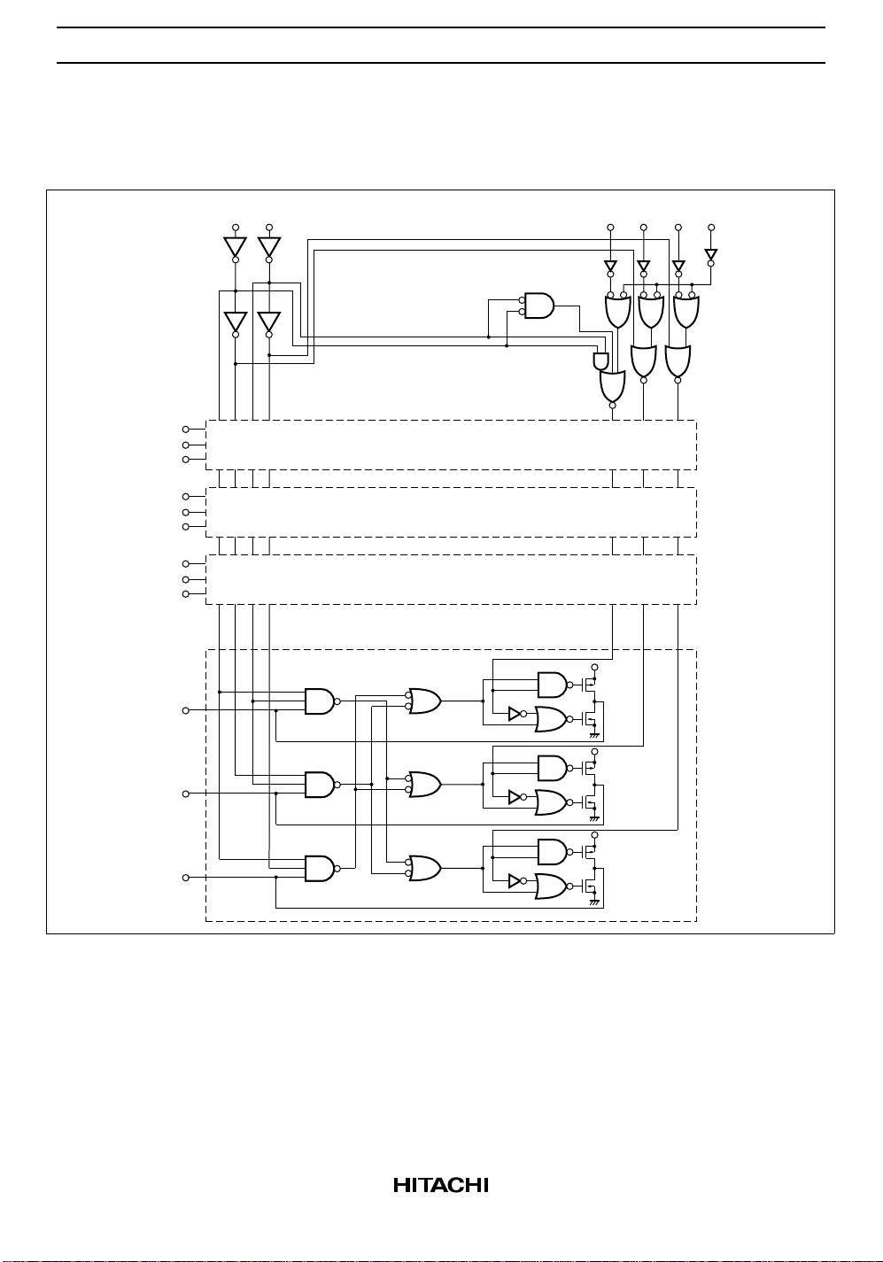
Logic Diagram
HD74HC442
S0
S1 GA GH GC CS
A1
B1
C1
A2
B2
C2
A3
B3
C3
A4
B4
C4
4
 Loading...