

HIT HD74HC4066 Datasheet
HD74HC4066
Quad Analog Switches/Quad Multiplexers
Description
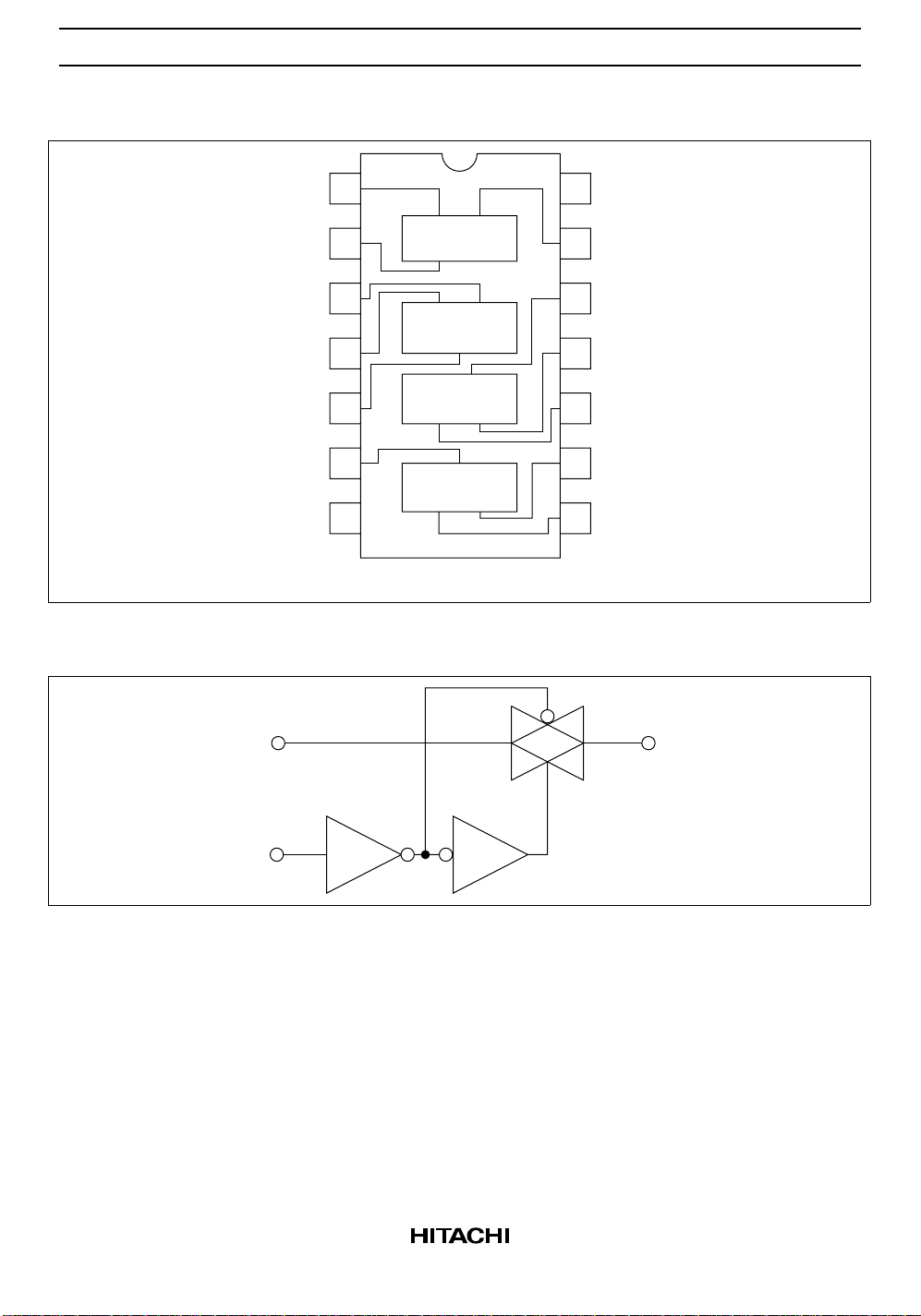
This switch has low “on” resistance and low “off” leakage. It is a bidirectional switch, thus any analog
input may be used as an output and vice-versa. Also the HD74HC4066 switch contains linearization
circuitry which lowers the “on” resistance and increases switch linearity. The HD74HC4066 device allows
control of up to 12 V (peak) analog signals with digital control signals of the same range. Each switch has
its own control input which disables each switch when low.
Features
• High Speed Operation
• Wide Operating Voltage
• Low Quiescent Supply Current
Function Table
Control Switch
L OFF
HON
GND ≤ Vin ≤ V
GND ≤ Vout ≤ V
CC
CC
HD74HC4066
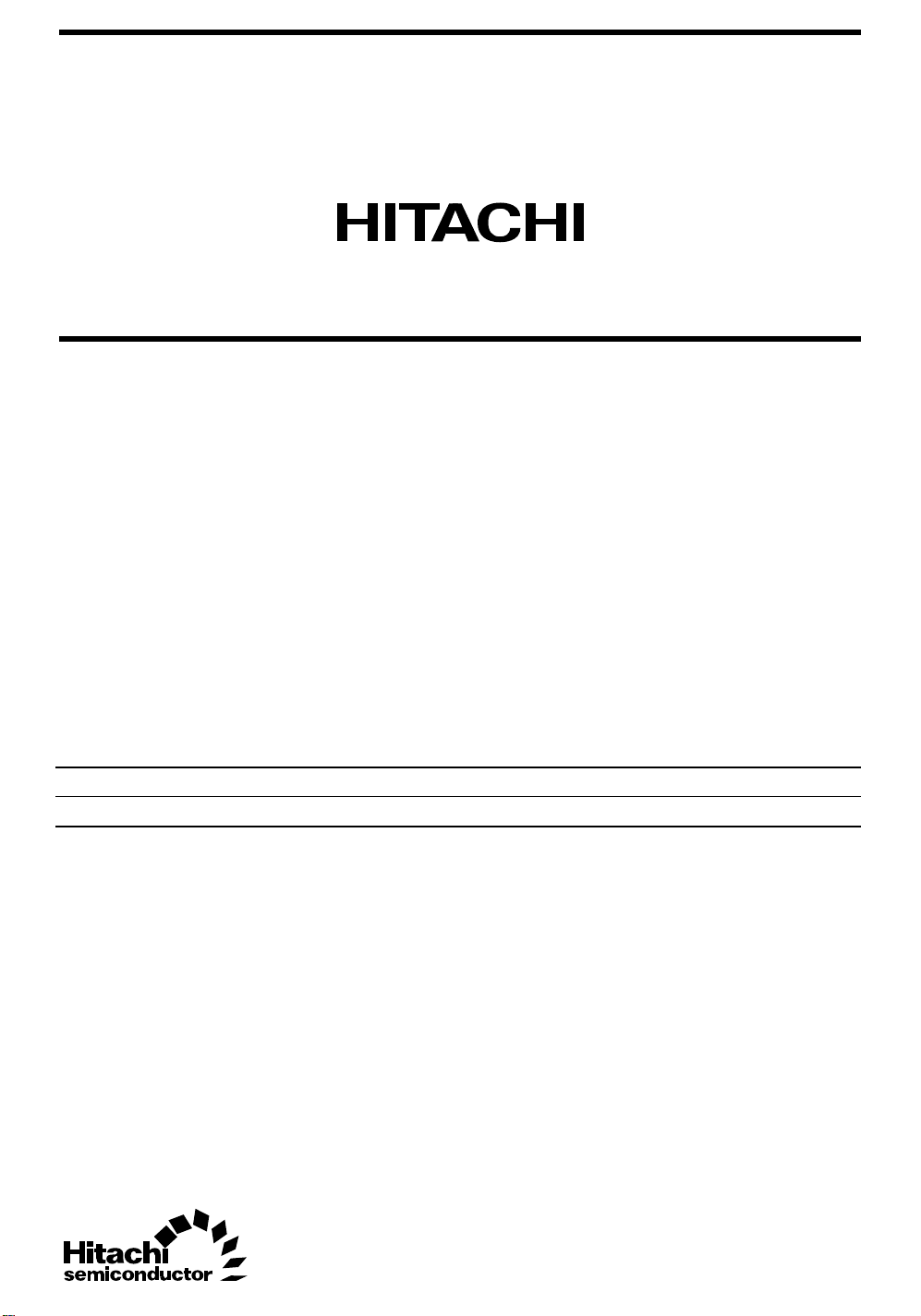
Pin Arrangement
Logic Diagram (1/4)
In 1
Out 1
Out 2
In 2
Control 2
Control 3
GND
1
In C
2
3
4
5
6
Out
In Out
C
C
Out In
C
In Out
7
14
13
12
11
10
9
8
V
CC
Control 1
Control 4
In 4
Out 4
Out 3
In 3
(Top view)
In/Out Out/In
Control
2
HD74HC4066
Absolute Maximum Ratings
Item Symbol Rating Unit
Supply voltage V
Control input voltage V
Switch I/O voltage V
Supply current (VCC)I
(GND) I
Switch I/O current (per pin) I
Control input diode current I
Switch I/O diode current I
Power dissipation P
CC
IN
I/O
CC
GND
I/O
IK
IOK
T
Storage temperature range Tstg –65 to +150 °C
–0.5 to +7.0 V
–0.5 to VCC + 0.5 V
–0.5 to VCC + 0.5 V
+50 mA
–50 mA
±25 mA
±20 mA
±20 mA
500 mW
3
 Loading...