HIT HD74HC4052 Datasheet

HD74HC4052/HD74HC4053
Dual 4-channel Analog Multiplexers/Demultiplexers/
Triple 2-channel Analog Multiplexers/Demultiplexers
Description
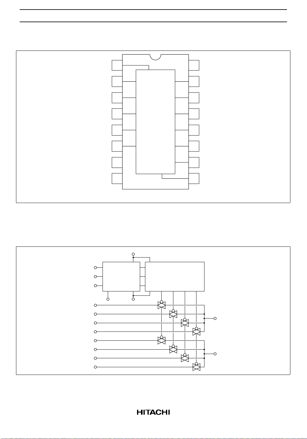
HD74HC4052: This device connects together the outputs of 4 switches in two sets, thus achieving a pair of
4 channel multiplexers. The binary code placed on the A, and B select lines determine which switch in
each 4 channel section is “on”, connecting one of the four inputs in each section to its common output.
This enables the implementation of a 4 channel differential multiplexer.
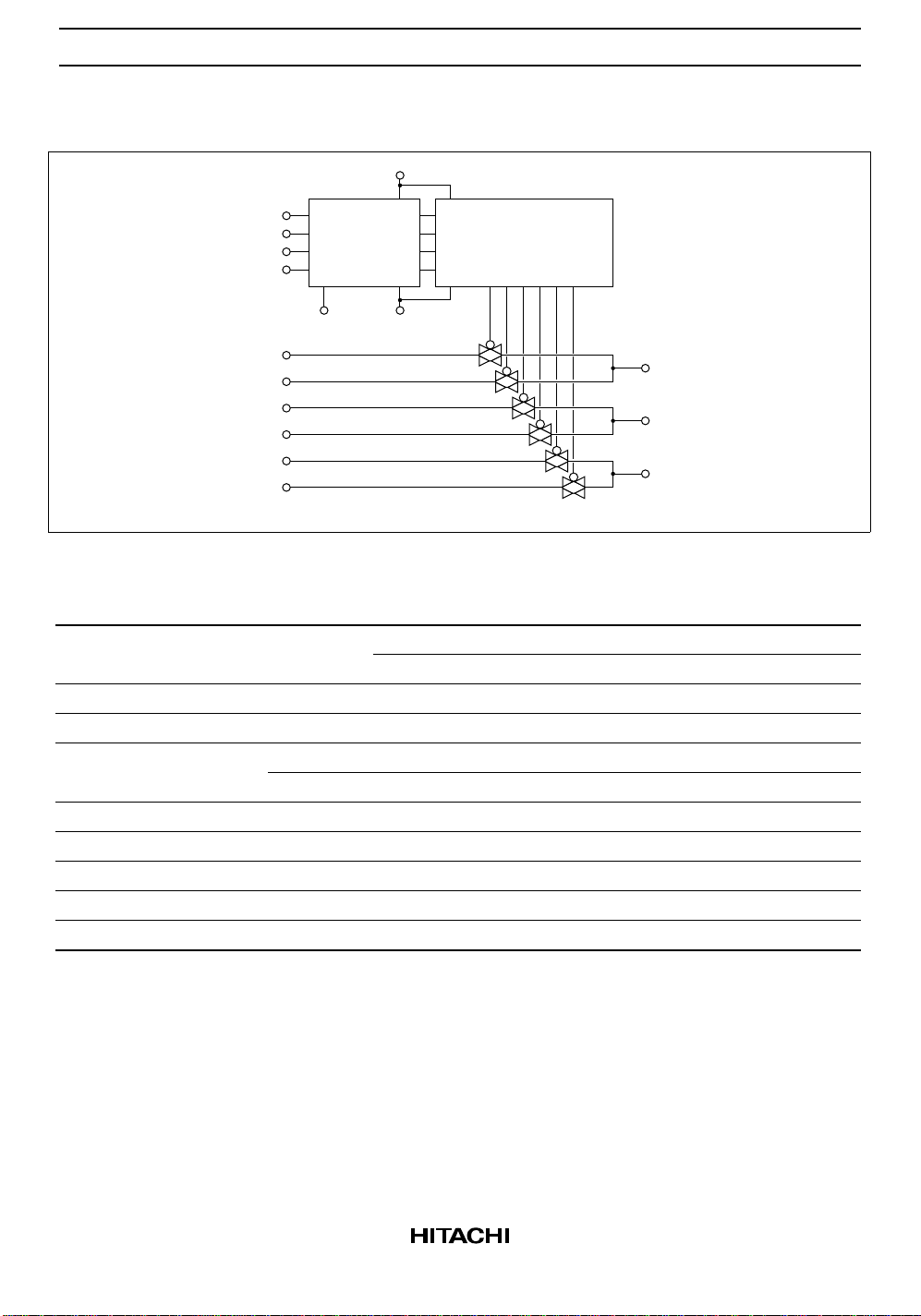
HD74HC4053: This device contains 6 switches whose outputs are connected together in pairs, thus
implementing a triple 2 channel multiplexer, or the equivalent of 3 single-pole-double throw configuration.
Each of the A, B, or C select lines independently controls one pair of switches, selecting one of the two
switches to be “on”.
Features
• High Speed Operation
• Wide Operating Voltage
• Low Quiescent Supply Current

HD74HC4052/HD74HC4053
Function Table
Control Inputs
Select ON Switch
Inhibit C*
LLLLY
LL L H Y
LL H L Y
LL HHY
LH L L Z
LH L H Z
LH H L Z
LH H H Z
HXXX— —
Note: 1. Not applicable for HD74HC4052
1
B A HD74HC4052 HD74HC4053
X = Dont’t Care
0
1
2
3
X
0
X
1
X
2
X
3
Z
0
Z
0
Z
0
Z
0
1
1
1
1
Y
0
Y
0
Y
1
Y
1
Y
0
Y
0
Y
1
Y
1
X
0
X
1
X
0
X
1
X
0
X
1
X
0
X
1
Pin Arrangement
HD74HC4052
Y
Y
Y
Y
Inhibit
V
EE
GND
1
0
Y
2
2
Y
3
4
3
5
1
6
Y
2
Y
Y
3
Y
1
Inhibit
7
0
X
2
X
1
X
X
0
X
3
A
16
15
14
13
12
11
10
V
CC
X
2
X
1
X
X
0
X
3
A
B
B
8
9
(Top view)
2

HD74HC4053
HD74HC4052/HD74HC4053
Block Diagram
HD74HC4052
Y
Y
Z
Z
Inhibit
V
EE
GND
1
1
Y
2
0
3
1
Z
4
5
0
6
Y
0
Z
1
Z
Z
0
Inhibit
7
1
Y
X
X
1
X
0
A
B
16
15
14
13
12
11
10
V
CC
Y
X
X
1
X
0
A
B
C
C
8
9
(Top view)
Inh
X
X
X
X
Y
Y
Y
Y
V
CC
A
B
0
1
2
3
0
1
2
3
Level
Converter
GND V
EE
Binary to
1-of-4 Decoder
with Inhibit
X
Y
3

HD74HC4052/HD74HC4053
HD74HC4053
V
CC
Inh
X
X
Y
Y
Z
Z
A
B
C
0
1
0
1
0
1
Level
Converter
GND V
EE
Binary to 1-of-2
Decoder with
Inhibit
X
Y
Z
Absolute Maximum Ratings
Item Symbol Rating Unit
Supply voltage V
Control input voltage V
Switch I/O voltage V
Supply current (VCC)I
(GND) I
Switch I/O current (per pin) I
Control input diode current I
Switch I/O diode current I
Power dissipation P
CC
VCC – V
IN
I/O
CC
GND
I/O
IK
IOK
T
EE
Storage temperature range Tstg –65 to +150 °C
–0.5 to +7.0 V
–0.5 to +7.0 V
GND – 0.5 to VCC + 0.5 V
VEE –0.5 to VCC + 0.5 V
+50 mA
–50 mA
±25 mA
±20 mA
±20 mA
500 mW
4

HD74HC4052/HD74HC4053
Recommended Operating Range
Item Symbol Min Typ Max Unit
Supply voltage V
CC
– V
GND – V
Control input voltage V
Switch I/O voltage V
IN
I/O
Operating temperature Topr –40 — +85 °C
Input rise/fall time VCC = 2.0 V tr, t
f
VCC = 4.5 V 0 — 500 ns
VCC = 6.0 V 0 — 400 ns
2—6V
EE
–4 — 0 V
EE
0—VCCV
V
EE
—VCCV
0 — 1000 ns
5
 Loading...