

HIT HD74HC4051 Datasheet
HD74HC4051
8-Channel Analog Multiplexer Demultiplexer
Description
This device connects together the outputs of 8 switches, thus achieving an 8 Channel Multiplexer. The
binary code placed on the A, B, and C select lines determine which one of the eight switches in “on”, and
connects one of the eight inputs to the common output.
Features
• High Speed Operation
• Wide Operating Voltage
• Low Quiescent Supply Current
Function Table
Control Inputs
Inhibit C B A ON Switch
LL L L X
LL L H X
LL H L X
LL H H X
LH L L X
LH L H X
LH H L X
LH H H X
HX X X —
X : Don’t Care
0
1
2
3
4
5
6
7

HD74HC4051
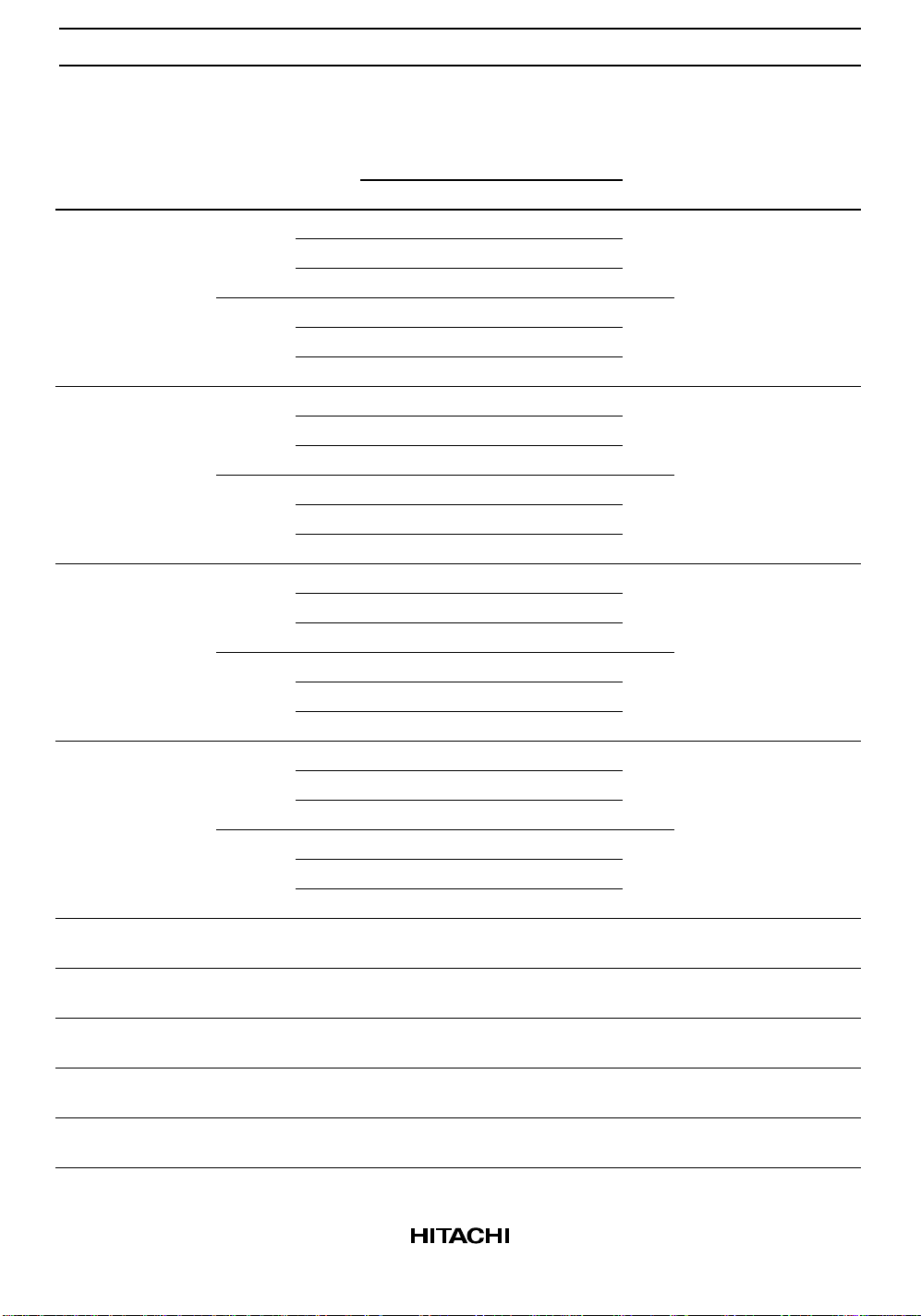
Pin Arrangement
Block Diagram
X
X
X
X
Inhibit
V
EE
GND
1
4
X
2
6
X
3
4
7
5
5
6
X
6
X
X
7
X
5
Inhibit
7
4
X
2
X
1
X
0
X
3
A
B
16
15
14
13
12
11
10
V
CC
X
2
X
1
X
0
X
3
A
B
C
C
8
9
(Top View)
V
CC
Control
Switch
In/Out
Inhibit
X
X
X
X
X
X
X
X
A
B
C
0
1
2
3
4
5
6
7
Level
Converter
GND V
EE
Binary to 1-of-8
Decoder With inhibit
Common
Out/In
X
2
HD74HC4051
Absolute Maximum Ratings
Item Symbol Rating Unit
Supply voltage V
Control input voltage V
Switch I/O voltage V
Supply current (VCC)I
(GND) I
Switch I/O current (per pin) I
Control input diode current I
Switch I/O diode current I
Power dissipation P
CC
VCC – V
IN
I/O
CC
GND
I/O
IK
IOK
T
EE
Storage temperature range Tstg –65 to +150 °C
Recommended Operating Range
–0.5 to +7.0 V
–0.5 to +7.0 V
GND – 0.5 to VCC + 0.5 V
V
– 0.5 to VCC + 0.5 V
EE
+50 mA
–50 mA
±25 mA
±20 mA
±20 mA
500 mW
Item Symbol Min Typ Max Unit
Supply voltage V
Control input voltage V
Switch I/O voltage V
– V
CC
V
– V
GND
IN
I/O
2—6V
EE
–4 — 0 V
EE
0—VCCV
V
EE
—VCCV
Operating temperature Topr –40 — +85 °C
Input rise/fall time VCC = 2.0 V tr, t
f
0 — 1000 ns
VCC = 4.5 V 0 — 500 ns
VCC = 6.0 V 0 — 400 ns
3

HD74HC4051
DC Characteristics (VSS = VEE = GND)
Ta = –40 to
Ta = 25°C
Item Symbol V
Control input voltage V
IH
(V) Min Typ Max Min Max Unit Test Conditions
CC
2.0 1.5 — — 1.5 — V
4.5 3.15 — — 3.15 —
6.0 4.2 — — 4.2 —
V
IL
2.0 — — 0.5 — 0.5 V
4.5 — — 1.35 — 1.35
6.0 — — 1.8 — 1.8
ON resistance R
ON
2.0 — 2000 5000 — 6250 Ω V
4.5 — 120 180 — 225 V
6.0 — 100 170 — 210 I
2.0 — 200 800 — 1000 Ω V
4.5 — 80 150 — 190 V
6.0 — 70 140 — 175 V
∆ON resistance ∆R
ON
2.0 —50———Ω V
between any two 4.5 — 13 40 — 50 V
channels 6.0 — 10 20 — 25 I
OFF channel
I
S (OFF)
6.0 — — ±0.1 — ±1.0 µAV
leakage current
(switch off)
OFF channel
I
S (ON)
6.0 — — ±0.1 — ±1.0 µAV
leakage current
(switch on)
Control input current Iin 6.0 — — ±0.1 — ±1.0 µA Vin = VCC or V
Quiescent supply
I
CC
6.0 — — 4.0 — 40 µA Vin = VCC or V
current
+85°C
= V
INH
= VCC to V
I/O
≤ 2 mA
I/O
= V
INH
= VCC to V
I/O
≤ 2 mA
I/O
= V
INH
= VCC to V
I/O
≤ 2 mA
I/O
= V
INH
= V
INH
IL
IL
IL
IL
IL
EE
EE
EE
SS
SS
4
HD74HC4051
AC Characteristics (CL = 50 pF, Input tr = tf = 6 ns, VSS = VEE = GND)
Ta = –40 to
Ta = 25°C
Item Symbol V
Propagation delay t
PLH
(V) Min Typ Max Min Max Unit Test Conditions
CC
2.0 — 25 60 — 75 ns RL = 10 kΩ
time 4.5 — 6 12 — 15 Switch input to
6.0 — 5 10 — 13 switch output
t
PHL
2.0 — 25 60 — 75 ns
4.5 — 6 12 — 15
6.0 — 5 10 — 13
Propagation delay t
PLH
2.0 — 50 153 — 191 ns RL = 10 kΩ
time 4.5 — 16 30 — 38 Control input to
6.0 — 14 26 — 33 switch output
t
PHL
2.0 — 50 153 — 191 ns
4.5 — 16 30 — 38
6.0 — 14 26 — 33
Output enable t
ZH
2.0 — 50 153 — 191 ns RL = 1 kΩ
time 4.5 — 14 30 — 38
6.0 — 12 26 — 33
t
ZL
2.0 — 50 153 — 191 ns
4.5 — 14 30 — 38
6.0 — 12 26 — 33
Output disable t
HZ
2.0 — 40 153 — 191 ns RL = 1 kΩ
time 4.5 — 17 30 — 38
6.0 — 14 26 — 33
t
LZ
2.0 — 40 153 — 191 ns
4.5 — 17 30 — 38
6.0 — 14 26 — 33
Control input
Cin — — 5 10 — 10 pF
capacitance
Switch input
Cin 5.0 — 5 — — — pF
capacitance
Output capacitance
Cout 5.0 — 22 — — — pF
(Common pin)
Feed through
Cin–out 5.0 — 0.7 — — — pF
capacitance
Power dissipation
C
PD
5.0 — 22.0 — — — pF
capacitance
+85°C
5
 Loading...