

HIT HD74HC377 Datasheet
HD74HC377
Octal D-type Flip-Flops (with Enable)
Description
Information at the D inputs meeting the setup time requirements is transferred to the Q outputs on the
positive-going edge of the clock pulse if the enable input G is low. Clock triggering occurs at a particular
voltage level and is not directly related to the transition time of the positive-going pulse. When the clock
input is at either the high or low level, the D input signal has no effect at the output. The circuits are
designed to prevent false clocking by transitions at the G input.
Features
• High Speed Operation: tpd = 13 ns typ (CL = 50 pF)
• High Output Current: Fanout of 10 LSTTL Loads
• Wide Operating Voltage: VCC = 2 to 6 V
• Low Input Current: 1 µA max
• Low Quiescent Supply Current: ICC (static) = 4 µA max (Ta = 25°C)
Function Table
Inputs Outputs
Enable G Clock Data Q Q
HX X Q
L HHL
L LLH
XLXQ
0
0
Q
0
Q
0
HD74HC377
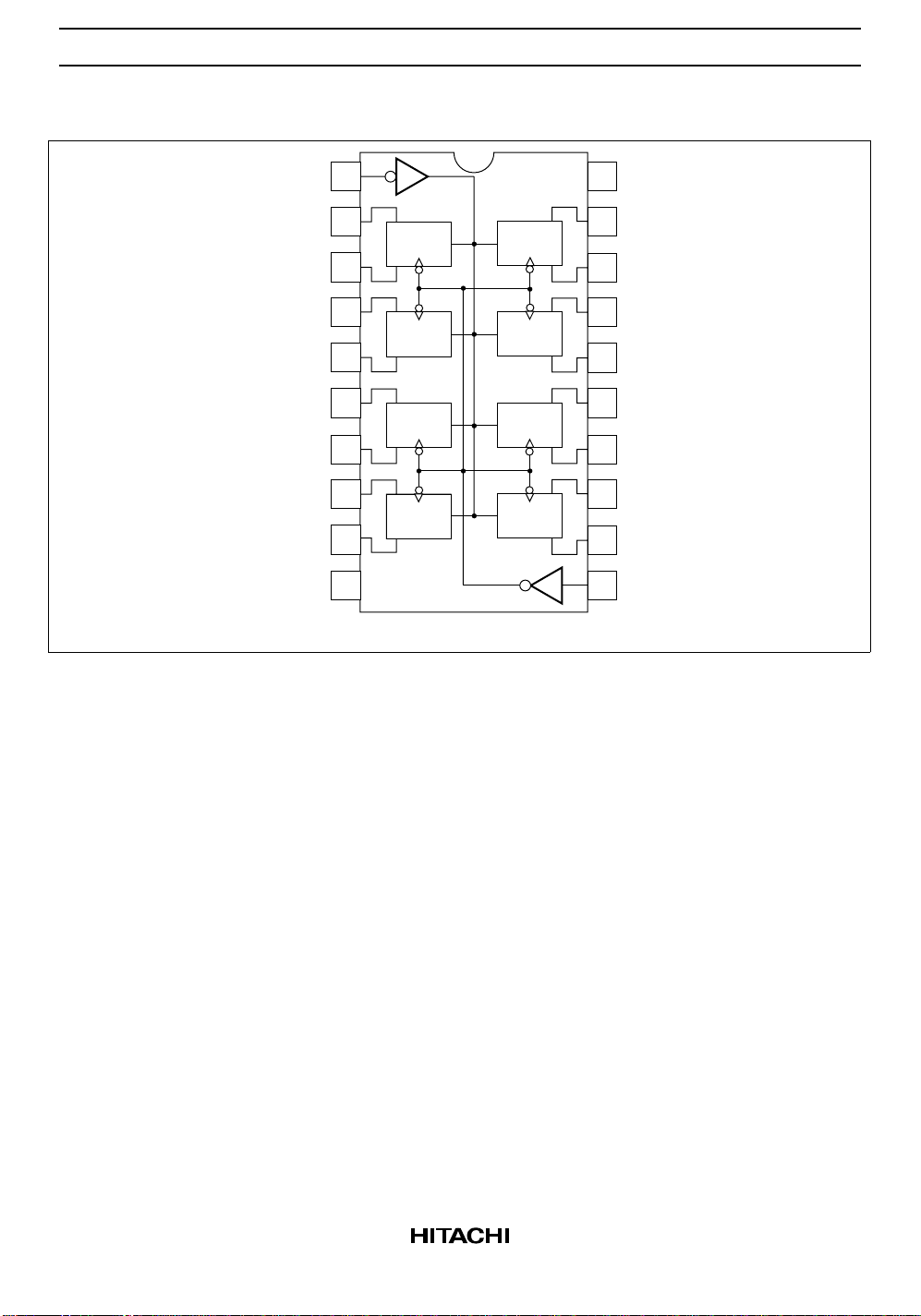
Pin Arrangement
Enable G
1Q
1D
2D
2Q
3Q
3D
4D
4Q
GND
1
2
Q
G
CK
D
3
4
D
CK
G
Q
5
6
Q
G
CK
D
7
8
D
CK
G
Q
9
10 11
(Top view)
G
CK
CK
G
G
CK
CK
G
20
19
Q
D
18
17
D
Q
16
15
Q
D
14
13
D
Q
12
VCC
8Q
8D
7D
7Q
6Q
6D
5D
5Q
Clock
2
HD74HC377
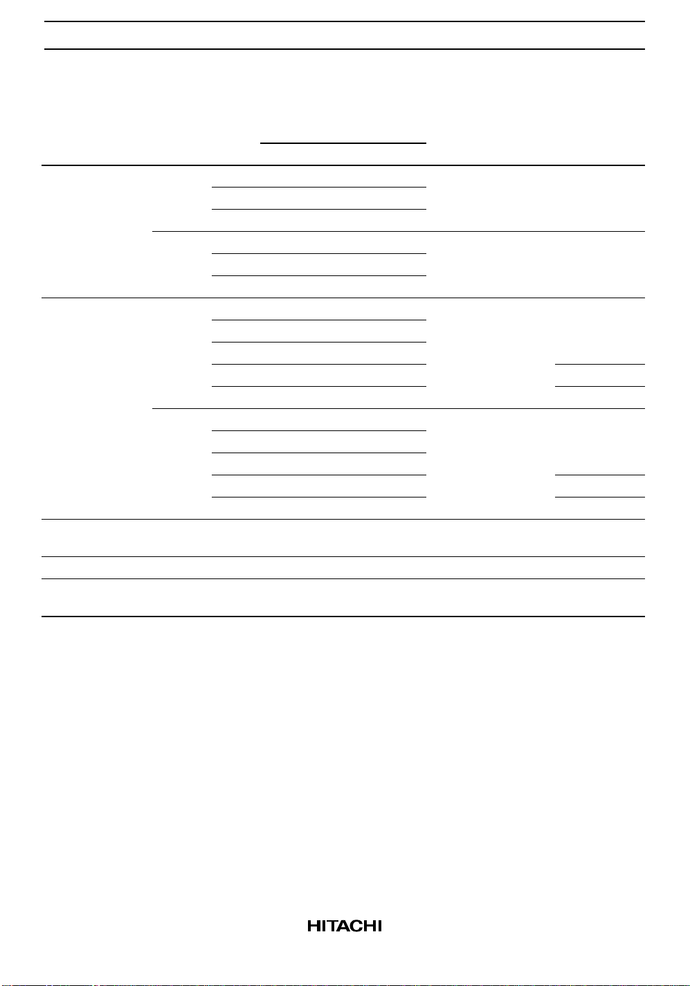
DC Characteristics
Ta = –40 to
Ta = 25°C
Item Symbol V
Input voltage V
IH
(V) Min Typ Max Min Max Unit Test Conditions
CC
2.0 1.5 — — 1.5 — V
4.5 3.15 — — 3.15 —
6.0 4.2 — — 4.2 —
V
IL
2.0 — — 0.5 — 0.5 V
4.5 — — 1.35 — 1.35
6.0 — — 1.8 — 1.8
Output voltage V
OH
2.0 1.9 2.0 — 1.9 — V Vin = VIH or VILIOH = –20 µA
4.5 4.4 4.5 — 4.4 —
6.0 5.9 6.0 — 5.9 —
4.5 4.18 — — 4.13 — IOH = –4 mA
6.0 5.68 — — 5.63 — IOH = –5.2 mA
V
OL
2.0 — 0.0 0.1 — 0.1 V Vin = VIH or VILIOL = 20 µA
4.5 — 0.0 0.1 — 0.1
6.0 — 0.0 0.1 — 0.1
4.5 — — 0.26 — 0.33 IOL = 4 mA
6.0 — — 0.26 — 0.33 IOL = 5.2 mA
Off-state output
I
OZ
6.0 — — ±0.5 — ±5.0 µA Vin = VIH or VIL,
current
Input current Iin 6.0 — — ±0.1 — ±1.0 µA Vin = VCC or GND
Quiescent supply
I
CC
6.0 — — 4.0 — 40 µA Vin = VCC or GND, Iout = 0 µA
current
+85°C
Vout = V
or GND
CC
3
 Loading...