HIT HD74HC374, HD74HC534 Datasheet

HD74HC374/HD74HC534
Octal D-type Flip-Flops (with 3-state outputs)
Octal D-type Flip-flops (with inverted 3-state outputs)
Description
These devices are positive edge triggered flip-flops. The difference between HD74HC374 and
HD74HC534 is only that the former is a true outputs and the latter is a false outputs. Data at the D inputs,
meeting the setup and hold time requirements, are transferred to the Q outputs on positive going transitions
of the clock (CK) input. When a high logic level is applied to the output control (OC) input, all outputs go
to a high impedance state, regardless of what signals are present at the other inputs and the state of the
storage elements.
Features
• High Speed Operation: tpd (Clock to Q) = 18 ns typ (CL = 50 pF)
• High Output Current: Fanout of 15 LSTTL Loads
• Wide Operating Voltage: VCC = 2 to 6 V
• Low Input Current: 1 µA max
• Low Quiescent Supply Current: ICC (static) = 4 µA max (Ta = 25°C)
Function Table
HD74HC374
Output Control Clock D
L
L LLH
L L X No change No change
HX X Z Z
X : irrelevant
Z : off (high-impedance) state of a 3-state output.
HHL
Q
HD74HC534
Q

HD74HC374/HD74HC534
Pin Arrangement
HD74HC374
HD74HC534
Out put
Control
1Q
1D
2D
2Q
3Q
3D
4D
4Q
GND
Out put
Control
1Q
1
2
3
4
5
6
7
8
9
10 11
(Top view)
1
2
20
19
18
17
16
15
14
13
12
20
19
CC
V
8Q
8D
7D
7Q
6Q
6D
5D
5Q
Clock
CC
V
8Q
1D
3
2D
4
2Q
5
3Q
6
3D
7
4D
8
9
4Q
GND
10 11
(Top view)
2
18
17
16
15
14
13
12
8D
7D
7Q
6Q
6D
5D
5Q
Clock

HD74HC374/HD74HC534
Absolute Maximum Ratings
Item Symbol Rating Unit
Supply voltage range V
Input voltage V
Output voltage V
DC current drain per pin I
DC current drain per VCC , GND ICC, I
DC input diode current I
DC output diode current I
Power Dissipation per package P
CC
IN
OUT
OUT
GND
IK
OK
T
Storage temperature Tstg –65 to +150 °C
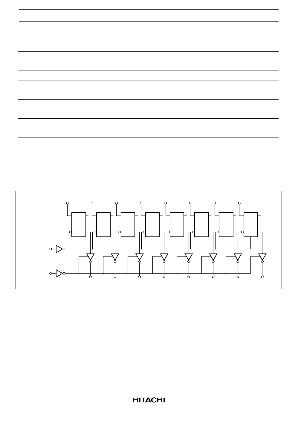
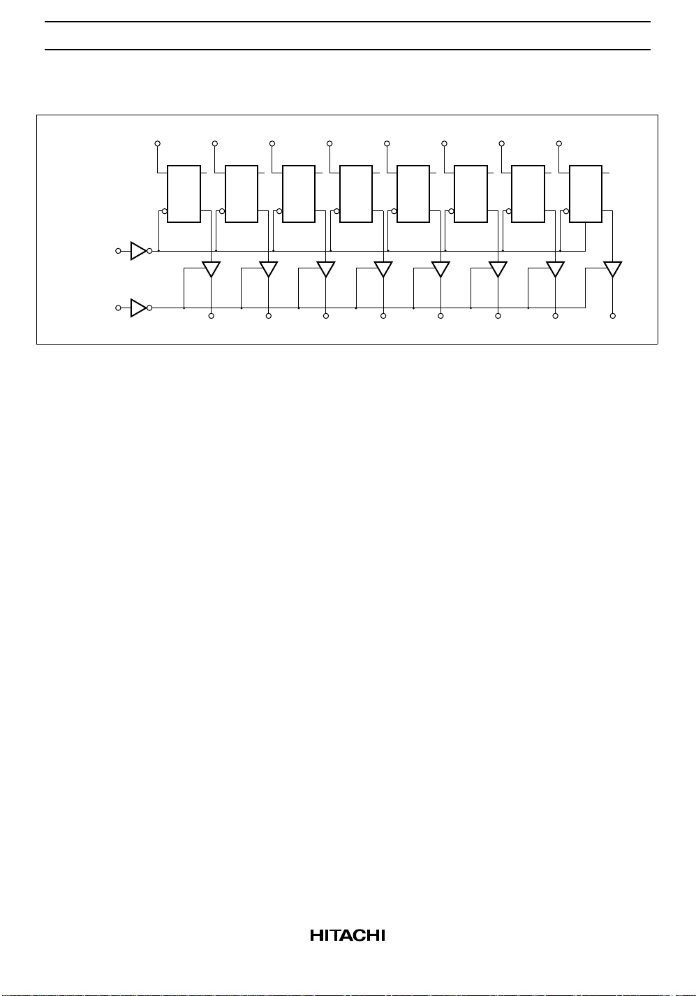
Block Diagram
HD74HC374
–0.5 to +7.0 V
–0.5 to VCC + 0.5 V
–0.5 to VCC + 0.5 V
±35 mA
±75 mA
±20 mA
±20 mA
500 mW
Clock
Output
Control
1D
2D
DQQQQQQQQ
Q
1Q
3D
D
Q
2Q
4D
D
Q
3Q
5D
D
Q
4Q
6D
D
Q
5Q
7D
D
Q
6Q
8D
D
CCCCCCC
D
Q
Q
C
7Q
8Q
3

HD74HC374/HD74HC534
HD74HC534
Clock
Output
Control
1D
2D
DQQQQQQQQ
Q
1Q
3D
D
Q
2Q
4D
D
Q
3Q
5D
D
Q
4Q
6D
D
Q
5Q
7D
D
Q
6Q
8D
D
CCCCCCC
D
Q
7Q
Q
C
8Q
4
 Loading...