HIT HD74HC356 Datasheet

HD74HC356
8-to-1-line Data Selectors/Multiplexer/Register
(with 3-state outputs)
Description
This data selectors/multiplexers contain full on-chip binary decoding to select one of eight data sources.
The data select address is stored in transparent latches that are enabled by a low level address on pin 11,
Select Control. Data on the 8 input lines is stored in a parallel input/output register which in the
HD74HC356 is composed of 8 edge-triggered flip-flops, clocked by a low to high transition on pin 9,
clock. Both true (Y) and complementary (W) 3-state outputs are available.
Features
• High Speed Operation: tpd (Clock to W, Y) = 27 ns typ (CL = 50 pF)
• High Output Current: Fanout of 15 LSTTL Loads
• Wide Operating Voltage: VCC = 2 to 6 V
• Low Input Current: 1 µA max
• Low Quiescent Supply Current: ICC (static) = 4 µA max (Ta = 25°C)

HD74HC356
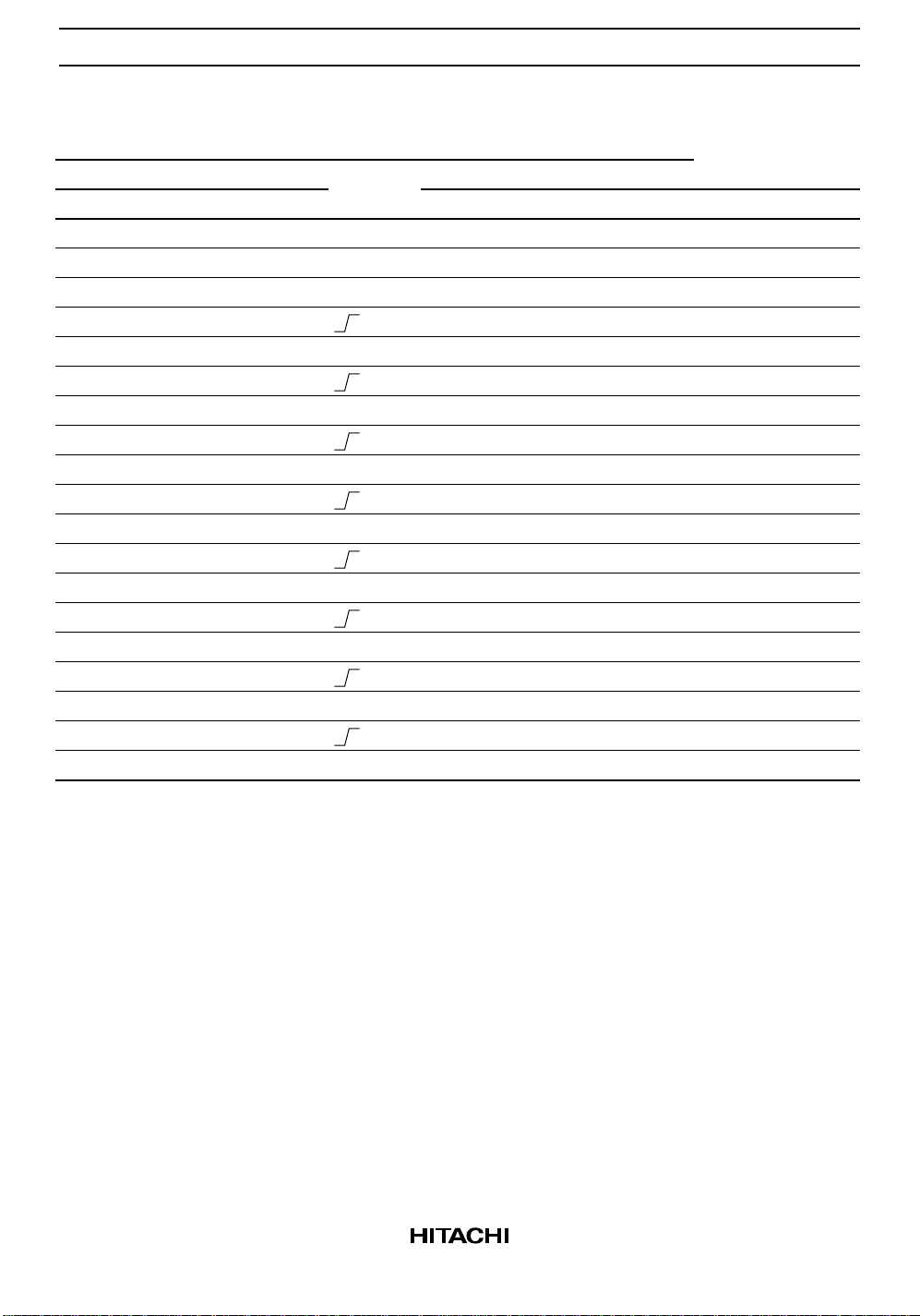
Function Table
Inputs
Select Output Enable Outputs
S
1
XXXXHXXZZ
XXXXXHXZZ
XXXXXXL ZZ
LLL LLHD
LLLH or LLLHD0nD
LLH LLHD
L L H H or L L L H D
LHL LLHD
LHLH or LLLHD2nD
LHH LLHD
L H H H or L L L H D
HLL LLHD
HLLH or LLLHD4nD
HLH LLHD
H L H H or L L L H D
HHL LLHD
HHLH or LLLHD6nD
HH H LLHD
H H H H or L L L H D
S
2
S
0
Clock G
1
G
2
G
3
WY
0
1
1n
2
3
3n
4
5
5n
6
7
7n
D
0
0n
D
1
D
1n
D
2
2n
D
3
D
3n
D
4
4n
D
5
D
5n
D
6
6n
D
7
D
7n
2

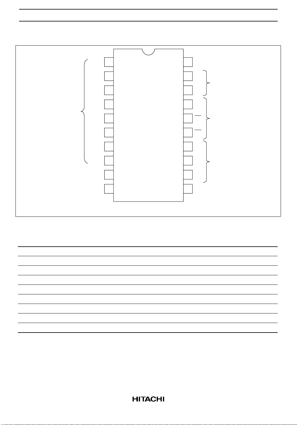
Pin Arrangement
HD74HC356
D
D
D
Data
inputs
D
D
D
D
D
Clock
GND
Absolute Masimum Ratings
1
7
2
6
20
19
V
CC
Y
Outputs
3
5
4
4
5
3
6
2
7
1
8
0
9
10
18
17
16
15
14
13
12
11
W
G
3
G
2
G
1
S
0
S
1
S
2
Select
control
Enables
Select
(Top view)
Item Symbol Rating Unit
Supply voltage range V
Input voltage V
Output voltage V
Output current I
CC
IN
OUT
OUT
DC current drain per VCC, GND ICC, I
DC input diode current I
DC output diode current I
Power dissipation per package P
IK
OK
T
GND
–0.5 to +7.0 V
–0.5 to VCC + 0.5 V
–0.5 to VCC + 0.5 V
±35 mA
±75 mA
±20 mA
±20 mA
500 mW
Storage temperature Tstg –65 to +150 °C
3
 Loading...