HIT HD74HC323 Datasheet

HD74HC323
8-bit Universal Shift/Storage Register (with 3-state Outputs)
Description
This eight-bit universal register features multiplexed I/O ports to achieve full eight bit data handling in a
single 20-pin package. HD74HC323 applications are as stacked or push-down registers, buffer storage, and
accumulator registers.
Two function-select inputs and two output control inputs can be used to choose the modes of operation
listed in the function table.
Synchronous parallel loading is accomplished by taking both function-select lines S0 and S1 high. This
places the three-state outputs in a high-impedance state, which permits data that is applied on the I/O ports
to be clocked into the register. Reading out of this register can be accomplished while the outputs are
enabled in any mode. The clear function is synchronous, and a low level at the clear input clears the
register on the next low-to-high transition of the clock.
Features
• High Speed Operation: tpd (Clock to Q) = 20 ns typ (CL = 50 pF)
• High Output Current: Fanout of 15 LSTTL Loads
• Wide Operating Voltage: VCC = 2 to 6 V
• Low Input Current: 1 µA max
• Low Quiescent Supply Current: ICC (static) = 4 µA max (Ta = 25°C)

HD74HC323
(
)
Function Table
Inputs
Function
Select
Mode Clear S1S0G1† G2† Clock SLSRA/QAB/QBC/QCD/QDE/QEF/QFG/QGH/QHQA’QH’
Clear L X L L L XXLLLLLLLLLL
LLXLL XXLLLLLLLLLL
Hold H LLLLX XXQA0QB0QC0QD0QE0QF0QG0QH0QA0Q
H XXLL L XXQA0QB0QC0QD0QE0QF0QG0QH0QA0Q
Shift H L H L L XHH QAnQBnQCnQDnQEnQFnQGnHQ
Right H L H L L XLL QAnQBnQCnQDnQEnQFnQGnLQ
Shift H H L L L HXQBnQCnQDnQEnQFnQGnQHnHQBnH
Left H H L L L LXQBnQCnQDnQEnQFnQGnQHnLQBnL
Load H H H X X XXabcdef ghah
a ... h = the level of the steady-state input at A through H, respectively. These data are loaded into the flipflops while the flip-flop outputs are isolated from the input/output terminals.
Output
Control Serial Inputs/Outputs Outputs
H0
H0
Gn
Gn
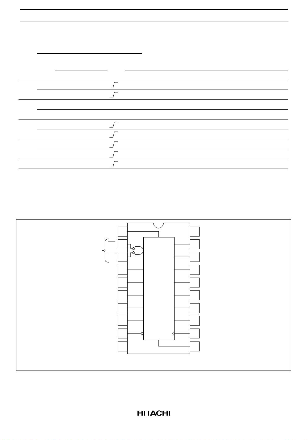
Pin Arrangement
Output
controls
S
G1
G
G/Q
E/Q
C/Q
A/Q
QA'
Clear
GND
1
1
0
S
0
2
2
G
3
3
2
4
4
C
5
5
E
6
6
C
7
7
A
8
8
9
9
10
10
G/Q
E/Q
C/Q
A/Q
Q
A
Clear
S
1
SL
Q
H
C
H/Q
H
E
F/Q
F
C
D/Q
D
A
B/Q
B
CK
SR
20
19
18
17
16
15
14
13
12
11
V
CC
S1
Shift left
SL
'
Q
H
H/Q
H
F/Q
F
D/Q
D
B/Q
B
Clock
Shift right
SR
Top view
2

HD74HC323
Absolute Maximum Ratings
Item Symbol Rating Unit
Supply voltage range V
Input voltage V
Output voltage V
Output current I
DC current drain per VCC, GND ICC, I
DC input diode current I
DC output diode current I
Power dissipation per package P
CC
IN
OUT
OUT
GND
IK
OK
T
Storage temperature Tstg –65 to +150 °C
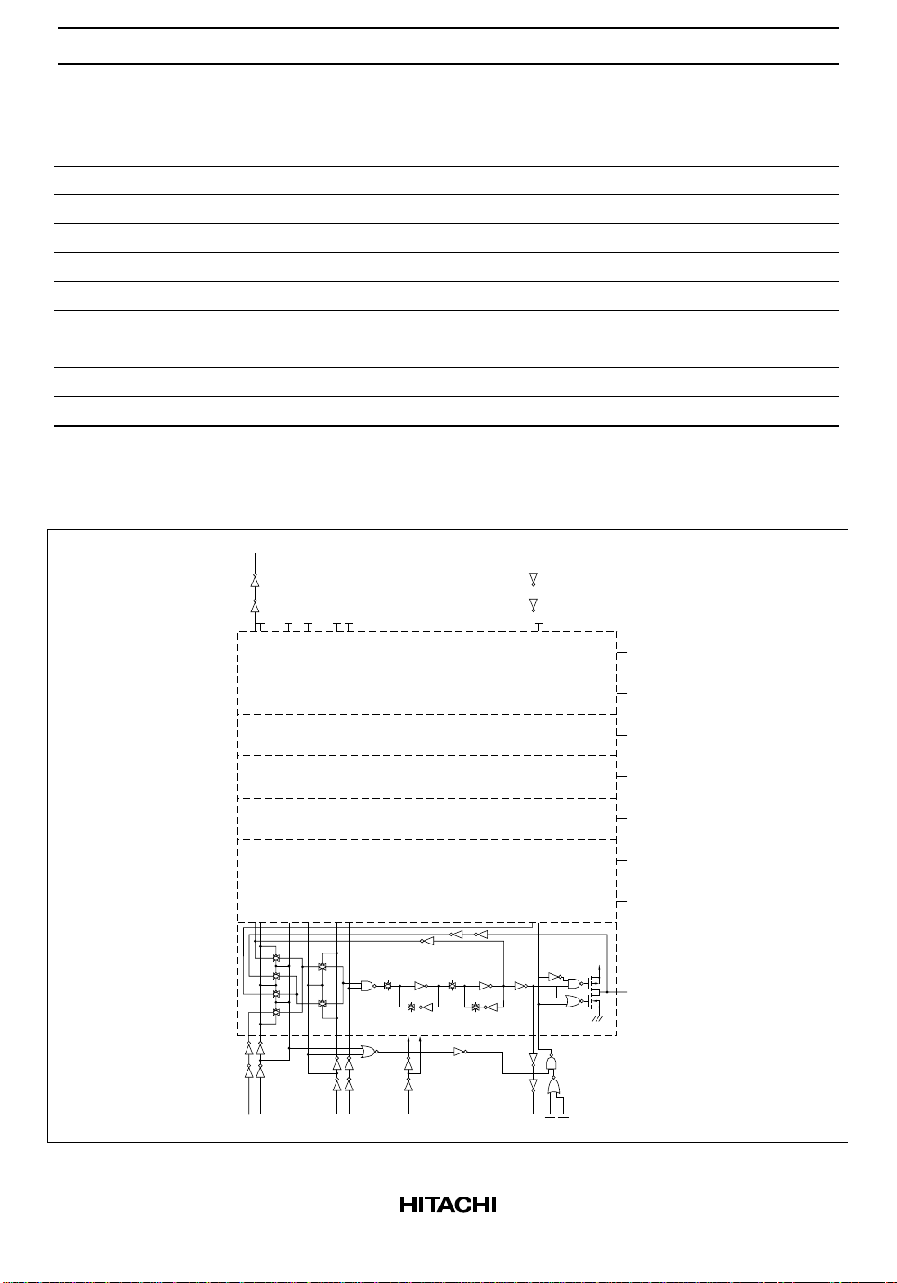
Logic Diagram
–0.5 to +7.0 V
–0.5 to VCC + 0.5 V
–0.5 to VCC + 0.5 V
±35 mA
±75 mA
±20 mA
±20 mA
500 mW
QH'
CK
CKCKCK
CK CK
SL
H/Q
H
G/Q
G
F/Q
F
E/Q
E
D/Q
D
C/Q
C
B/Q
B
CK
CK CK
CK
A/Q
A
S
0
S
ClearSR Clock
1
QA'
G
G
2
1
3
 Loading...