HIT HD74HC294, HD74HC292 Datasheet

HD74HC292/HD74HC294
Programmable Frequency Divider/Digital Timer
Description
This device divides the incoming clock frequency by a number (a power of 2) that is preset by the
Programming inputs. It has two Clock inputs, either of which may be used as a clock inhibit. The device
also has an active-low Reset, which initializes the internal flip-flop states. Test Point outputs (TP1, TP2,
TP3) are provided with HD74HC292 to facilitate incoming inspections.
Test Point output is provided with HD74HC294 to facilitate incoming inspections.
Features
• High Speed Operation: tpd (Clock to Q) = 16 ns typ (CL = 50 pF)
• High Output Current: Fanout of 10 LSTTL Loads
• Wide Operating Voltage: VCC = 2 to 6 V
• Low Input Current: 1 µA max
• Low Quiescent Supply Current: ICC (static) = 4 µA max (Ta = 25°C)
Function Table
CLR CLK1 CLK2 Q Output Mode
L X X Cleared to L
H L Count
HL Count
H H X Inhibit
H X H Inhibit

HD74HC292/HD74HC294
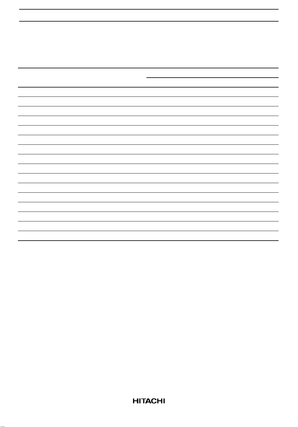
HD74HC292
Programming
Inputs Frequency Division
Q Out TP1 TP2 TP3
E D C B A Binary Decimal Binary Decimal Binary Decimal Binary Decimal
L L L L L Inhibit Inhibit Inhibit Inhibit Inhibit Inhibit Inhibit Inhibit
L L L L H Inhibit Inhibit Inhibit Inhibit Inhibit Inhibit Inhibit Inhibit
L LLHL 2
L LLHH 2
LLHLL 2
LLHLH 2
LLHHL 2
LLHHH 2
LHLLL 2
LHLLH 2
LHLHL 2
LHLHH 2
L HHL L 2
L HHL H 2
L HHHL 2
L HHHH 2
HLLLL 2
HLLLH 2
HLLHL 2
HLLHH 2
HLHLL 2
HLHLH 2
HLHHL 2
HLHHH 2
HHLLL 2
HHLLH 2
HHLHL 2
2
3
4
5
6
7
8
9
10
11
12
13
14
15
16
17
18
19
20
21
22
23
24
25
26
1,048,576 2
2,097,152 2
4,194,304 Disabled LOW 2
8,388,608 Disabled LOW 2
16,777,216 2
33,554,432 2
67,108,864 2
429512 2
829512 2
16 2
32 2
64 2
128 2
256 2
512 2
1,024 2
2,048 2
4,096 2
8,192 2
16,384 2
32,768 2
65,536 2
131,072 2
262,144 2
524,288 2
HHLHH 227134,217,728 2
H HHL L 228268,435,456 2
H HHL H 229536,870,912 2
H HHHL 2301,073,741,824 2
H HHHH 2312,147,483,648 2
9
512 2
9
512 2
9
512 2
9
512 2
9
512 2
9
512 2
9
512 2
9
512 2
9
512 2
9
512 2
9
512 Disabled LOW 2
9
512 Disabled LOW 2
9
512 2
9
512 2
9
512 2
9
512 2
9
512 2
9
512 2
3
3
5
5
7
7
9
9
82112,048 2
82112,048 2
32 2
32 2
128 2
128 2
512 2
512 2
17
131,072 22416,777,216
17
131,072 22416,777,216
17
131,072 22416,777,216
17
131,072 22416,777,216
17
131,072 22416,777,216
17
131,072 22416,777,216
17
131,072 2
17
131,072 2
17
131,072 2
17
131,072 2
17
131,072 2
17
131,072 2
3
3
5
5
7
7
9
9
13
13
15
15
17
17
82101,024
82101,024
32 2
32 2
128 2
128 2
512 2
512 2
8,192 2
8,192 2
32,768 2
32,768 2
131,072 22416,777,216
131,072 22416,777,216
2
2
4
4
6
6
8
8
12
12
14
14
16
16
18
18
20
20
22
22
16
16
64
64
256
256
4,096
4,096
16,384
16,384
65,536
65,536
262,144
262,144
1,048,576
1,048,576
4,194,304
4,194,304
4
4
2

HD74HC292/HD74HC294
HD74HC294
Programming Inputs Frequency Division
Q Output TP Output
D C B A Binary Decimal Binary Decimal
L L L L Inhibit Inhibit Inhibit Inhibit
L L L H Inhibit Inhibit Inhibit Inhibit
LL H L 2
LL H H 2
LH L L 2
LH L H 2
LH H L 2
LH H H 2
HL L L 2
HL L H 2
2
3
4
5
6
7
8
9
42
82
16 2
32 2
64 2
128 Disabled LOW
256 2
512 2
HL H L 2101,024 2
HL H H 2112,048 2
HH L L 2124,096 2
HH L H 2138,192 2
HH H L 21416,384 2
HH H H 21532,768 2
9
9
9
9
9
2
3
4
5
6
7
8
9
512
512
512
512
512
16
32
64
128
256
512
4
8
3

HD74HC292/HD74HC294
R
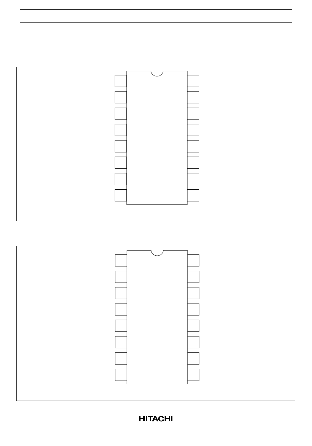
Pin Arrangement
HD74HC292
HD74HC294
TP1
CLK1
CLK2
TP2
GND
1
B
2
E
3
4
5
6
7
Q
8
(Top view)
1
B
16
15
14
13
12
11
10
16
V
CC
C
D
TP3
NC
CL
A
9
NC
V
CC
2
A
3
TP
NC
4
5
6
7
Q
8
(Top view)
CLK1
CLK2
GND
4
15
14
13
12
11
10
C
D
NC
NC
CLR
NC
9
NC
 Loading...