

HIT HD74HC279 Datasheet
HD74HC279
Quad. S–R Latches
Description
The latch is ideally suited for use as temporary stage for binary information processing and input/output
units. When either S or R is low, output is dependent on R input. When both inputs are high, Output is
stored before the indicated steady-state input conditions were established. And when both inputs are low,
output is high, but this high level are uncontinuance, if either of input goes high.
Features
• High Speed Operation: tpd (S to Q) = 10 ns typ (CL = 50 pF)
• High Output Current: Fanout of 10 LSTTL Loads
• Wide Operating Voltage: VCC = 2 to 6 V
• Low Input Current: 1 µA max
• Low Quiescent Supply Current: ICC (static) = 2 µA max (Ta = 25°C)
Function Table
Input Output
2
S*
HH Q
LH H
HL L
LL H*
H : High level
L : Low level
Q
: The level of Q respectively, before the indicated steady-state input conditions were established.
0
Notes: 1. It is unpredictable, if S or R goes High.
2. As to latches which has two S inputs.
H: Both of S inputs are high.
L: Either or both of S inputs are low.
R Q
0
1
HD74HC279
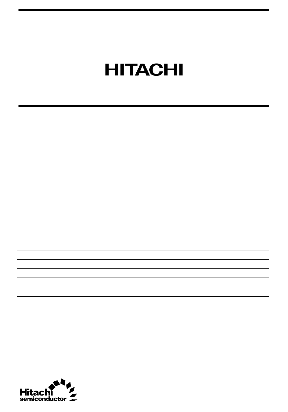
Pin Arrangement
1R
1
16
V
CC
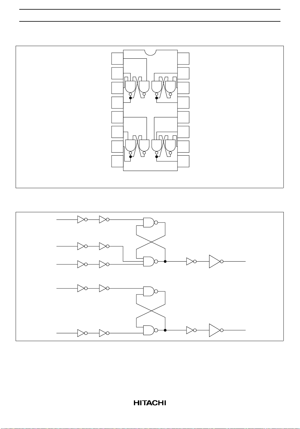
Logic Diagram (1/2)
R
S
1
1S1
1S2
1Q
2R
2S
2Q
GND
2
3
4
5
6
7
8
(Top view)
15
14
13
12
11
10
4S
4R
4Q
3S2
3S1
3R
3Q
9
S
2
R
S
2
Q
Q
HD74HC279
DC Characteristics
Ta = –40 to
Ta = 25°C
Item Symbol V
Input voltage V
IH
(V) Min Typ Max Min Max Unit Test Conditions
CC
2.0 1.5 — — 1.5 — V
4.5 3.15 — — 3.15 —
6.0 4.2 — — 4.2 —
V
IL
2.0 — — 0.5 — 0.5 V
4.5 — — 1.35 — 1.35
6.0 — — 1.8 — 1.8
Output voltage V
OH
2.0 1.9 2.0 — 1.9 — V Vin = VIH or VILIOH = –20 µA
4.5 4.4 4.5 — 4.4 —
6.0 5.9 6.0 — 5.9 —
4.5 4.18 — — 4.13 — IOH = –4 mA
6.0 5.68 — — 5.63 — IOH = –5.2 mA
V
OL
2.0 — 0.0 0.1 — 0.1 V Vin = VIH or VILIOL = 20 µA
4.5 — 0.0 0.1 — 0.1
6.0 — 0.0 0.1 — 0.1
4.5 — — 0.26 — 0.33 IOL = 4 mA
6.0 — — 0.26 — 0.33 IOL = 5.2 mA
Input current Iin 6.0 — — ±0.1 — ±1.0 µA Vin = VCC or GND
Quiescent supply
I
CC
6.0 — — 2.0 — 20 µA Vin = VCC or GND, Iout = 0 µA
current
+85°C
3
 Loading...