HIT HD74HC194 Datasheet

HD74HC194
4-bit Bidirectional Universal Shift Register
Description
This bidirectional shift register is designed to incorporate virtually all of the features a system designer may
want in a shift register. It features parallel inputs, parallel outputs, right shift and left shift serial inputs,
operating mode control inputs, and a direct overriding clear line. The register has four distinct modes of
operation: parallel (broadside) load, shift right (in the direction QA toware QD); shift left; inhibit clock (do
nothing).
Synchronous parallel loading is accomplished by applying the four bits of data and taking both mode
control inputs, S0 and S1, high. The data are loaded into their respective flip-flops and appear at the outputs
after the positive transition of the clock input. During loading, serial data flow is inhibited. Shift right is
accomplished synchronously with the rising edge of the clock pulse when S0 is high and S1 is low. Serial
data for this mode is entered at the shift right data input. When S0 is low and S1 is high, data shifts left
synchronously and new data is entered at the shift left serial input. Clocking of the flip-flops is inhibited
when both mode control inputs are low. The mode control inputs should be changed only when the clock
input is high.
Features
• High Speed Operation: tpd (Clock to Q) = 12 ns typ (CL = 50 pF)
• High Output Current: Fanout of 10 LSTTL Loads
• Wide Operating Voltage: VCC = 2 to 6 V
• Low Input Current: 1 µA max
• Low Quiescent Supply Current: ICC (static) = 4 µA max

HD74HC194
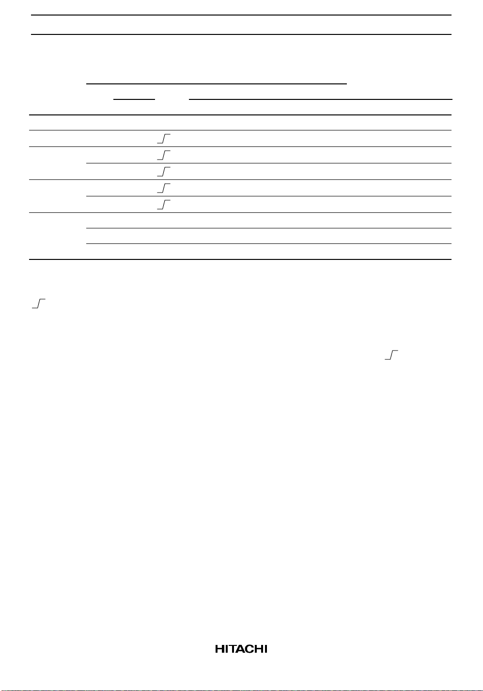
Function Table
Inputs
Operating Mode Serial Parallel Outputs
Mode Clear S1S0Clock Shift Left Shift Right A B C D QAQBQCQ
Clear L X X X X X X X X X LLLL
Parallel load H H H X X abcdabcd
Shift right H L H X H XXXXH QAnQBnQ
HLH X L XXXXL QAnQBnQ
Shift left H H L H X XXXXQBnQCnQDnH
HHL L X XXXXQBnQCnQDnL
Hold H L L X X X X X X X QA0QB0QC0Q
H X X L X X XXXXQA0QB0QC0Q
H X X H X X XXXXQA0QB0QC0Q
H : high level (Steady state)
L : low level (Steady state)
X : don’t care
: transition from low to high level.
a, b, c, d : the level of steady-state input at inputs A, B, C or D respectively.
QA0, QB0, QC0, QD0: the level of QA, QB, QC or QD respectively, before the indicated steady-state input
conditions were established.
, QBn, QCn, QDn: the level of QA, QB, QC or QD respectively before the most recent transition of
Q
An
the clock.
D
Cn
Cn
D0
D0
D0
2

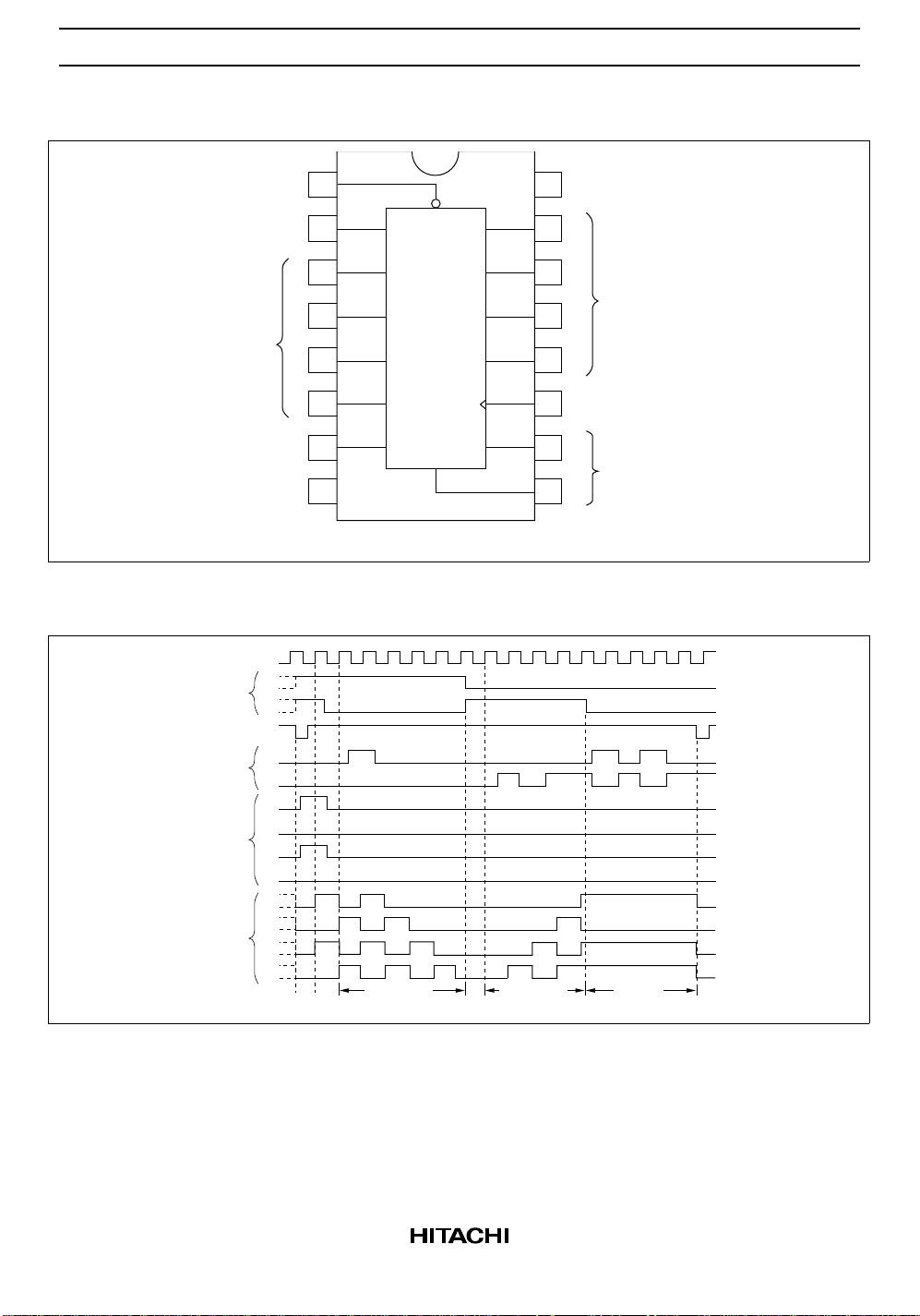
Pin Arrangement
HD74HC194
Timing Diagram
Mode
Control
Inputs
Serial
Data
Inputs
Parallel
Data
Inputs
Outputs
Clear
Shift
Right
Serial-Input
Parallel
Inputs
Shift
Left
Serial-Input
GND
Clock
0
S
S1
Clear
R
L
A
B
C
D
A
Q
QB
QC
QD
Clear ClearLoad
A
B
C
D
1
2
3
CLR
R
A
QA
QB
16
15
14
V
QA
QB
CC
Parallel
4
5
6
7
B
C
D
L
S0
QC
QD
CK
S
1
8
13
12
11
10
9
Outputs
QC
QD
Clock
S
1
Mode Control
S0
(Top view)
H
L
H
L
Shift Right Shift Left Inhibit
3
 Loading...