HIT HD74HC173 Datasheet

HD74HC173
4-bit D-type Register (with 3-state Outputs)
Description
The four D type Flip-Flops operate synchronously from a common clock. The 3-state outputs allow the
device to be used in bus organized systems. The outputs are placed in the 3-stage mode when either of the
output disable pins are in the logic high level.
The input disable allows the flip-flops to remain in their present states without having to disrupt the clock.
If either of the 2 input disables are taken to a logic high level, the Q outputs are fed back to the inputs,
forcing the flip-flops to remain in the same state. Clearing is enabled by taking the clear input to a logic
high level. The data outputs change state on the positive going edge of the clock.
Features
• High Speed Operation: tpd (Clock to Q) = 14 ns typ (CL = 50 pF)
• High Output Current: Fanout of 10 LSTTL Loads
• Wide Operating Voltage: VCC = 2 to 6 V
• Low Input Current: 1 µA max
• Low Quiescent Supply Current: ICC (static) = 4 µA max (Ta = 25°C)
Function Table
Inputs
Data Enable
Clear Clock G
HXXXXL
LLXXXQ
L HXXQ
L XHXQ
L LLLL
L LLHH
Note: When either M or N (or both) is (are) high the output is disabled to the high-impedance state;
however sequential operation of the flip-flops is not affected.
1
G
2
Data D Output Q
0
0
0

HD74HC173
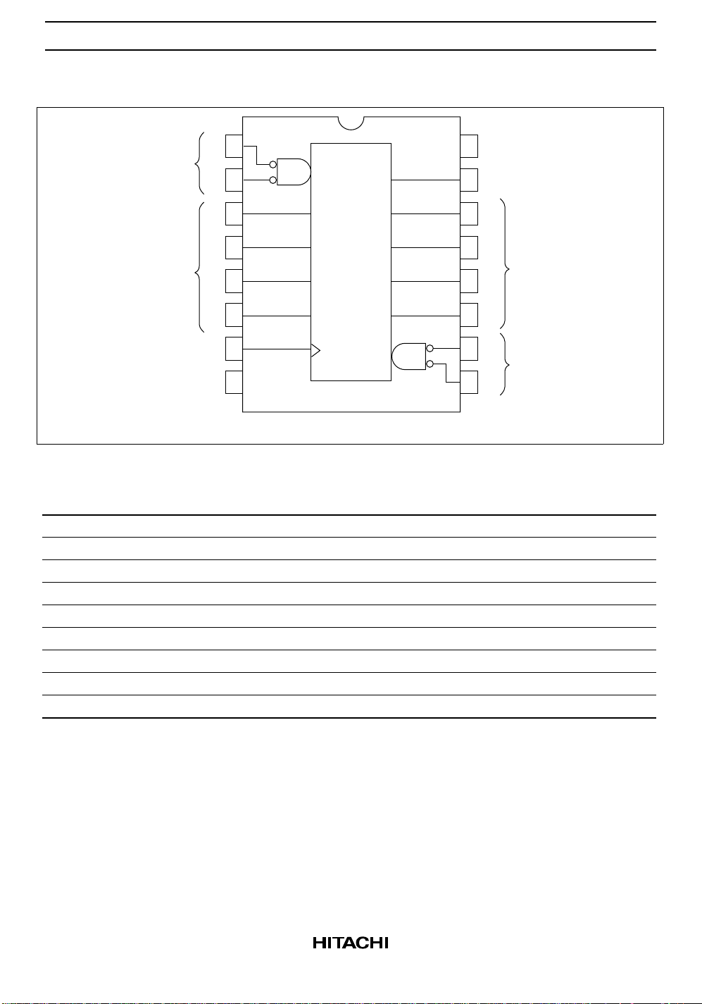
Pin Arrangement
Output
Control
Output
1Q
2Q
3Q
4Q
Clock
GND
1
M
Output
2
N
3
4
5
6
Control
1Q
2Q
3Q
4Q
7
CK
Clear
1D
2D
3D
4D
Data
Enable
8
16
15
14
13
12
11
10
9
V
CC
Clear
1D
2D
3D
4D
2
G
G1
Data
Input
Data
Enable
Input
(Top view)
Absolute Maximum Ratings
Item Symbol Rating Unit
Supply voltage range V
Input voltage V
Output voltage V
DC current drain per pin I
DC current drain per VCC, GND ICC, I
DC input diode current I
DC output diode current I
Power dissipation per package P
CC
IN
OUT
OUT
GND
IK
OK
T
Storage temperature Tstg –65 to +150 °C
–0.5 to +7.0 V
–0.5 to VCC + 0.5 V
–0.5 to VCC + 0.5 V
±35 mA
±75 mA
±20 mA
±20 mA
500 mW
2

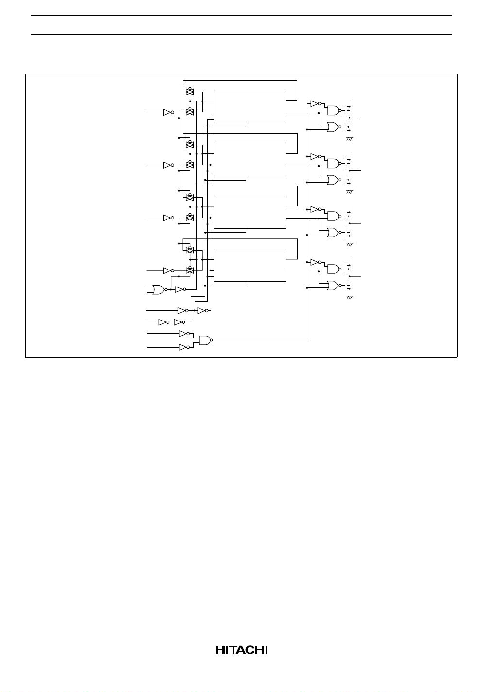
Block Diagram
1D
2D
3D
4D
G
G2
HD74HC173
V
DQ
C
R
C
DQ
C
R
C
DQ
C
R
C
DQ
C
R
1
C
Q
Q
Q
Q
CC
1Q
V
CC
2Q
V
CC
3Q
V
CC
4Q
Clock
Clear
Control M
Control N
3
 Loading...