HIT HD74HC164 Datasheet

HD74HC164
8-bit Parallel-out Shift Register
Description
This 8-bit shift register has gated serial inputs and clear. Each register bit is a D-type master/slave flipflop. Inputs A & B permit complete control over the incoming data. A low at either or both inputs inhibits
entry of new data and resets the first flip-vlop to the low level at the next clock pulse. A high level on the
input enables the other input which will then determine the state of the first flip-flop. Data at the serial
inputs may be changed while the clock is high or low, but only information meeting the setup and hold time
requirements will be entered. Data is serially shifted in and out of the 8-bit register during the positive
going transition of the clock pulse. Clear is independent of the clock and accomplished by a low level at
the clear input.
Features
• High Speed Operation: tpd (Clock to Q) = 14.5 ns typ (CL = 50 pF)
• High Output Current: Fanout of 10 LSTTL Loads
• Wide Operating Voltage: VCC = 2 to 6 V
• Low Input Current: 1 µA max
• Low Quiescent Supply Current: ICC (static) = 4 µA max
Function Table
Inputs Outputs
Clear Clock A B Q
L X X X L L ········· L
H XXQAoQ
H LXLQAn········· Q
H XL LQAn········· Q
H HHHQAn········· Q
QAo to QHo = Outputs remain unchanged.
Q
to QGn = Data shifted from the previous stage on a positive edge at the clock input.
An
A
Q
B
Bo
········· Q
········· Q
H
Ho
Gn
Gn
Gn

HD74HC164
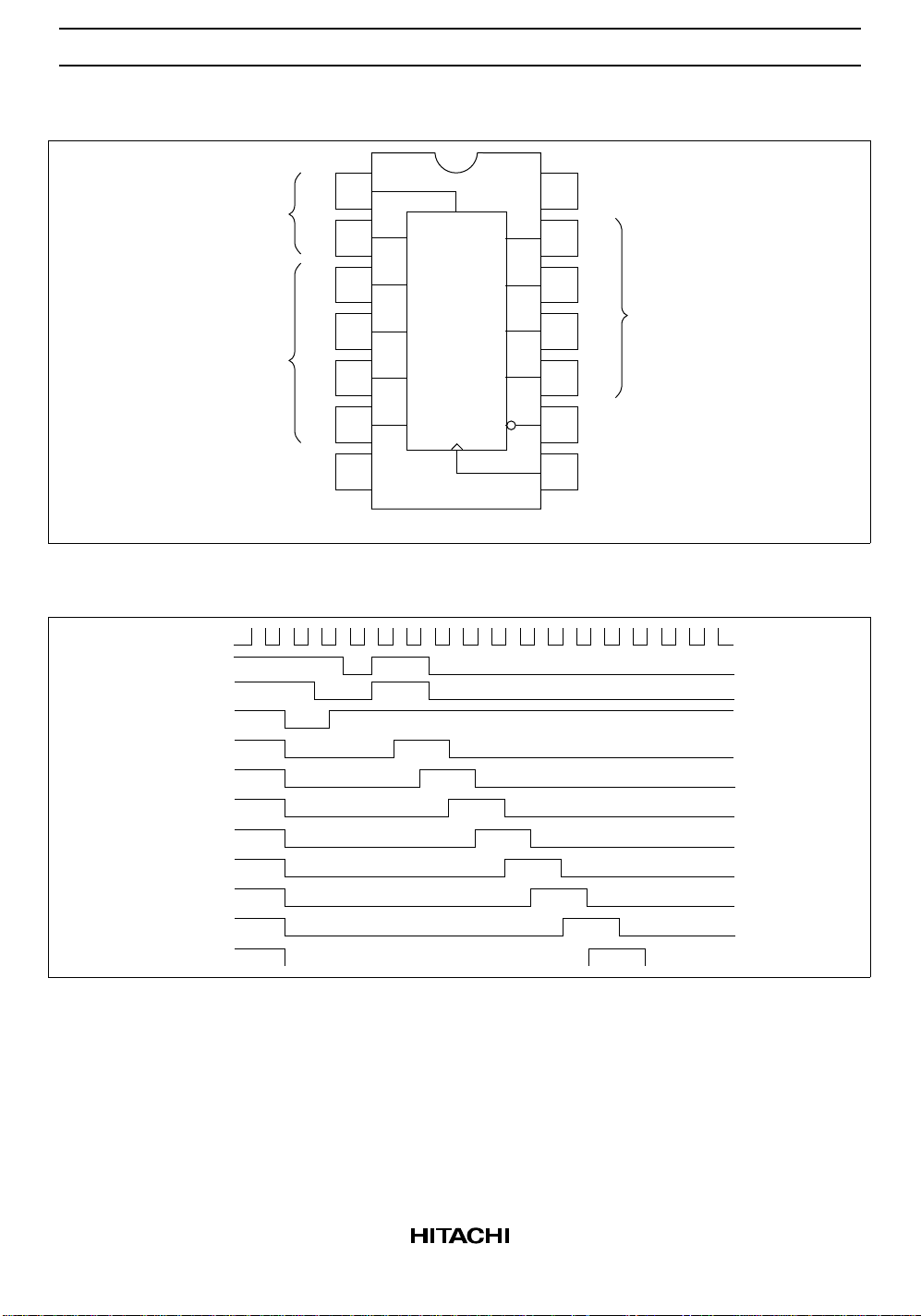
Pin Arrangement
Serial
Inputs
Outputs
QA
QB
QC
1
A
A
2
B
3
4
5
B
Q
QB
QC
A
QH
QG
QF
QE
14
13
12
11
10
V
QH
QG
QF
QE
CC
Outputs
Timing Diagram
Clock
Clear
QG
QH
Q
QB
QC
QD
QE
QF
6
QD
7
GND
A
B
A
QD
CLR
CK
(Top view)
Clear
9
Clock
8
2

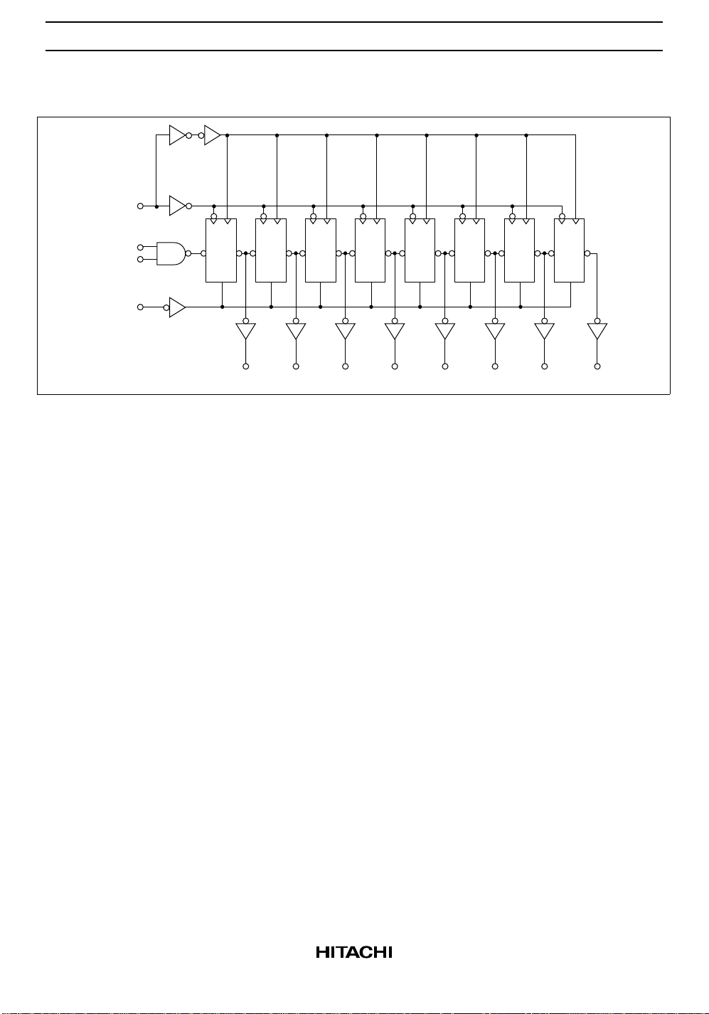
Logic Diagram
Clock
HD74HC164
Clear
A
B
DQ DQ DQ DQDQ DQ DQ DQ
CLR
CLR CLR CLR CLR CLR CLR CLR
QA QB QC QD QE QF QG QH
3
 Loading...