HIT HD74HC109 Datasheet

HD74HC109
Dual J-K Flip-Flops (with Preset and Clear)
Description
Each flip-flop has independent J, K, preset, clear and clock inputs and Q and Q outputs. This device is
edge sensitive to the clock input and changes state on the positive going transition of the clock pulse. Clear
and preset are independent of the clock and accomplished by a low logic level on the corresponding input.
Features
• High Speed Operation: tpd (Clock to Q) = 15 ns typ (CL = 50 pF)
• High Output Current: Fanout of 10 LSTTL Loads
• Wide Operating Voltage: VCC = 2 to 6 V
• Low Input Current: 1 µA max
• Low Quiescent Supply Current: ICC (static) = 2 µA max (Ta = 25°C)
Function Table
Inputs Output
Preset Clear Clock J K Q Q
LHXXXHL
HLXXXL H
LLXXXH*
HH LLLH
HH H L Toggle
HH LHQ
HH HHHL
HHLXXQ
Note: 1. Q and Q will remain high as long as preset and clear input are low, but Q and Q are
unpredictable if preset and clear input go high simultaneously.
1
0
0
1
H*
Q
0
Q
0

HD74HC109
(
)
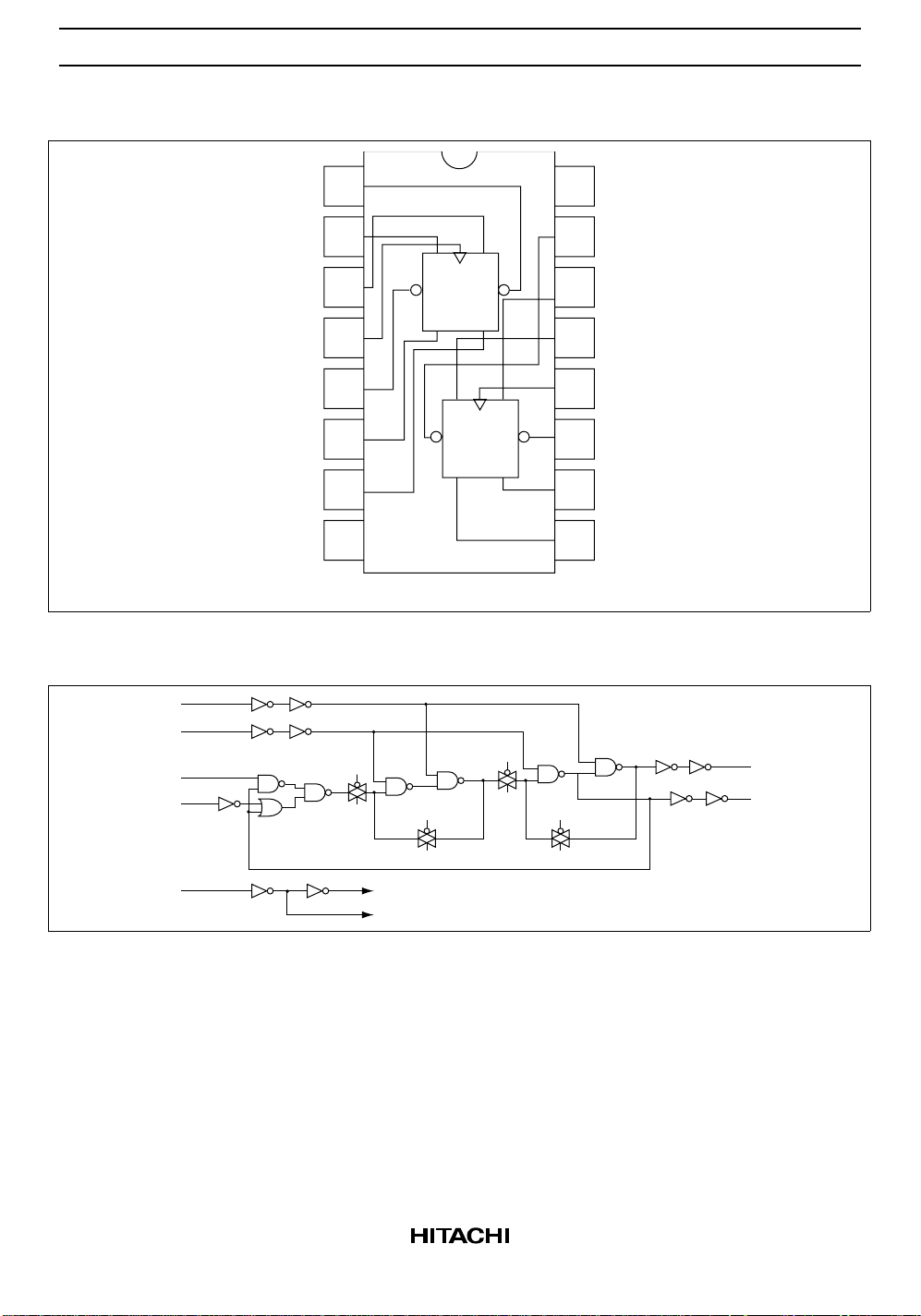
Pin Arrangement
Block Diagram (1/2)
PR
CLR
J
K
1CLR
1
21J
J K
31K
CK
CLRPR
16
V
CC
2CLR15
2J14
Q Q
41CK
51PR
K J
61Q
CK
PRCLR
2K13
2CK12
2PR11
Q Q
71Q
8GND
2Q10
2Q9
Top view
C
C
C
C
C
C
Q
Q
C
CK
C
C
C
2

HD74HC109
DC Characteristics
Ta = –40 to
Ta = 25°C
Item Symbol V
Input voltage V
IH
(V) Min Typ Max Min Max Unit Test Conditions
CC
2.0 1.5 — — 1.5 — V
4.5 3.15 — — 3.15 —
6.0 4.2 — — 4.2 —
V
IL
2.0 — — 0.5 — 0.5 V
4.5 — — 1.35 — 1.35
6.0 — — 1.8 — 1.8
Output voltage V
OH
2.0 1.9 2.0 — 1.9 — V Vin = VIH or VILIOH = –20 µA
4.5 4.4 4.5 — 4.4 —
6.0 5.9 6.0 — 5.9 —
4.5 4.18 — — 4.13 — IOH = –4 mA
6.0 5.68 — — 5.63 — IOH = –5.2 mA
V
OL
2.0 — 0.0 0.1 — 0.1 V Vin = VIH or VILIOL = 20 µA
4.5 — 0.0 0.1 — 0.1
6.0 — 0.0 0.1 — 0.1
4.5 — — 0.26 — 0.33 IOL = 4 mA
6.0 — — 0.26 — 0.33 IOL = 5.2 mA
Input current Iin 6.0 — — ±0.1 — ±1.0 µA Vin = VCC or GND
Quiescent supply
I
CC
6.0 — — 2.0 — 20 µA Vin = VCC or GND, Iout = 0 µA
current
+85°C
3
 Loading...