HIT HD74CDCV857 Datasheet

HD74CDCV857
2.5-V Phase-lock Loop Clock Driver
ADE-205-335C (Z)
Preliminary
4th Edition
March 2000
Description
The HD74CDCV857 is a high-performance, low-skew, low-jitter, phase locked loop clock driver. It is
specifically designed for use with DDR (Double Data Rate) synchronous DRAMs.
Features
• Supports 60 MHz to 200 MHz operation range
• Distributes one differential clock input pair to ten differential clock outputs pairs
• Supports spread spectrum clock requirements meeting the PC100 SDRAM registered DIMM
specification
• External feedback pins (FBIN, FBIN) are used to synchronize the outputs to the clock input
• Supports 2.5V analog supply voltage (AVCC), and 2.5 V V
• No external RC network required
• Sleep mode detection
• 48pin TSSOP (Thin Shrink Small Outline Package)
DDQ

HD74CDCV857
Function Table
Inputs : Outputs : PLL
AV
GND H L H : L H L H : Bypassed / off
GND H H L : H L H L : Bypassed / off
XL LH: ZZZZ:off
XL HL: ZZZZ:off
2.5 V H L H : HL HL:on
2.5 V H H L : HL HL:on
2.5 V X 0 MHz 0 MHz : ZZZZ:off
H : High level
L : Low level
X : Don’t care
Z : High impedance
Note: 1. Bypasse mode is used for Hitachi test mode.
PWRDWN CLK CLK : Y Y FBOUT FBOUT
CC
*1
*1
2

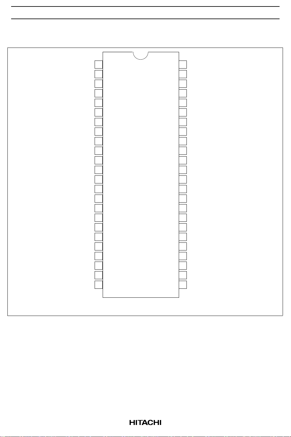
Pin Arrangement
N
GND
Y0
Y0
V
DDQ
Y1
Y1
GND
GND
Y2
Y2
V
DDQ
V
DDQ
CLK
CLK
V
DDQ
AV
CC
AGND
GND
Y3
Y3
V
DDQ
Y4
Y4
GND
10
11
12
13
14
15
16
17
18
19
20
21
22
23
24
HD74CDCV857
GND
1
2
3
4
5
6
7
8
9
48
47
46
45
44
43
42
41
40
39
38
37
36
35
34
33
32
31
30
29
28
27
26
25
Y5
Y5
V
DDQ
Y6
Y6
GND
GND
Y7
Y7
V
DDQ
PWRDW
FBIN
FBIN
V
DDQ
FBOUT
FBOUT
GND
Y8
Y8
V
DDQ
Y9
Y9
GND
(Top view)
3

HD74CDCV857
CC
CC
Pin Function
Pin name No. Type Description
AGND 17 Ground Analog ground. AGND provides the ground reference for the
analog circuitry.
AV
CC
CLK, CLK 13, 14 I
FBIN, FBIN 35, 36 I
FBOUT, FBOUT 32, 33 O
PWRDWN 37 I Output bank enable. PWRDWN is the output enable for all
GND 1, 7, 8, 18,
V
DDQ
Y 3, 5, 10, 20,
Y 2, 6, 9, 19,
16 Power Analog power supply. AVCC provides the power reference for
the analog circuitry. In addition, AV
the PLL for test purposes. When AV
can be used to bypass
is strapped to ground,
PLL is bypassed and CLK is buffered directly to the device
outputs. This bypass mode is used for Hitachi test.
Clock input. CLK provides the clock signal to be distributed by
Differential
input
the HD74CDCV857 clock driver. CLK is used to provide the
reference signal to the integrated PLL that generates the clock
output signals. CLK must have a fixed frequency and fixed
phase for the PLL to obtain phase lock. Once the circuit is
powered up and a valid CLK signal is applied, a stabilization
time is required for the PLL to phase lock the feedback signal to
its reference signal.
Feedback input. FBIN provides the feedback signal to the
Differential
input
internal PLL. FBIN must be hard-wired to FBOUT to complete
the PLL. The integrated PLL synchronizes CLK and FBIN so
that there is nominally zero phase error between CLK and
FBIN.
Feedback output. FBOUT is dedicated for external feedback. It
Differential
output
switches at the same frequency as CLK. When externally wired
to FBIN, FBOUT completes the feedback loop of the PLL.
outputs. When PWRDWN is low, VCO will stop and all outputs
are disabled to a high impedance state. When PWRDWN will
be returned high, PLL will re-synchroniz to CLK frequency and
all outputs are enabled.
Ground Ground
24, 25, 31,
41, 42, 48
4, 11, 12,
Power Power supply
15, 21, 28,
34, 38, 45
22, 27, 29,
39, 44, 46
23, 26, 30,
40, 43, 47
O
Differential
output
O
Differential
output
Clock outputs. These outputs provide low-skew copies of CLK.
Clock outputs. These outputs provide low-skew copies of CLK.
4

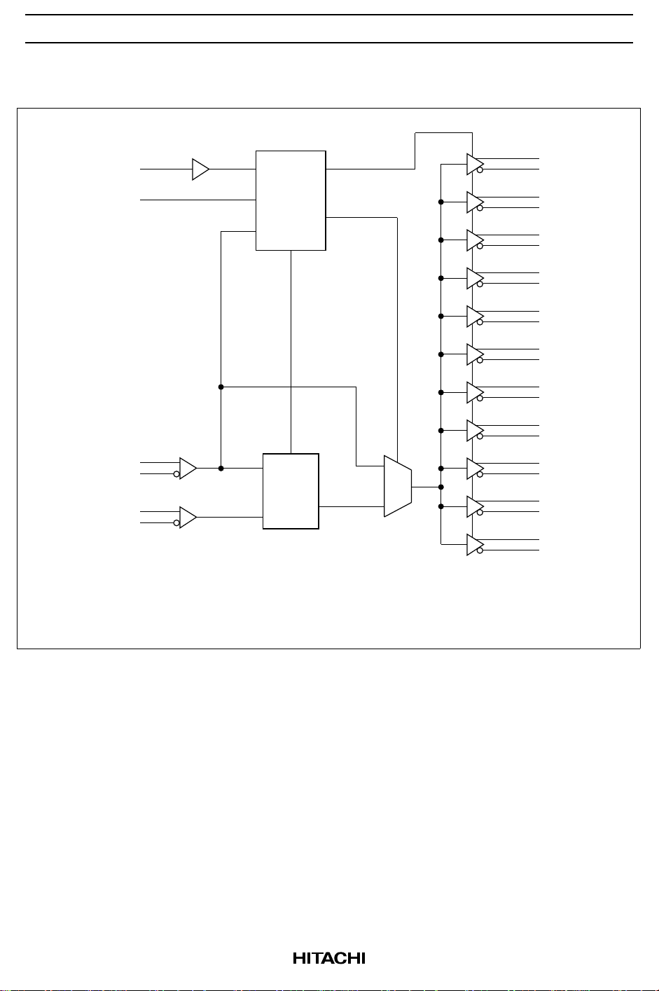
Logic Diagram
PWRDWN
AV
CC
CLK
CLK
FBIN
FBIN
HD74CDCV857
3
Y0
37
16
Powerdown
and Test
Logic
13
14
PLL
36
35
2
5
6
10
9
20
19
22
23
46
47
44
43
39
40
29
30
27
26
32
33
Y0
Y1
Y1
Y2
Y2
Y3
Y3
Y4
Y4
Y5
Y5
Y6
Y6
Y7
Y7
Y8
Y8
Y9
Y9
FBOUT
FBOUT
Note: All inputs and outputs are associated with V = 2.5 V.
DDQ
5
 Loading...