HIT HD74BC623A Datasheet

HD74BC623A
Octal Bus Transceivers With 3 State Outputs
ADE-205-025 (Z)
Rev.0
June 1993
Description
The HD74BC623A provides high drivability and operation equal to or better than high speed bipolar
standard logic IC by using Bi-CMOS process. The device features low power dissipation that is about 1/5
of high speed bipolar logic IC. When the frequency is 10 MHz. The device has eight bus transceivers with
three state outputs in a 20 pin package. This device allows data transmission from the A bus to the B bus or
from the B bus to the A bus depending upon the logic levels at the enable inputs (GBA and GAB). The
enable inputs can be used to disable the device so that the buses are effectively isolated.
Features
• Input/Output are at high impedance state when power supply is off.
• Input pins can be open, when not used, owing to built in input pull up circuit.
• Input is TTL level.
• Wide operating temperature range
Ta = –40 to +85°C.
Function Table
Enable Inputs
GBA GAB Operation
L L B data to A bus
H H A data to B bus
H L Isolation
L H B data to A bus
A data to B bus
H : High level
L : Low level

HD74BC623A
Pin Arrangement
GAB
A1
A2
A3
A4
A5
A6
A7
A8
GND
10
1
2
3
4
5
6
7
8
9
20
19
18
17
16
15
14
13
12
11
V
CC
GBA
B1
B2
B3
B4
B5
B6
B7
B8
(Top view)
Absolute Maximum Ratings
Item Symbol Rating Unit
Supply voltage V
Input diode current I
Input voltage V
Output voltage V
Off state output voltage V
CC
IK
IN
OUT
OUT(off)
Storage temperature Tstg –65 to +150 °C
Note: 1. The absolute maximum ratings are values which must not individually be exceeded, and
furthermore, no two of which may be realized at the same time.
–0.5 to +7.0 V
±30 mA
–0.5 to +7.5 V
–0.5 to +7.5 V
–0.5 to +5.5 V
2

HD74BC623A
Recommended Operating Conditions
Item Symbol Min Typ Max Unit
Supply voltage V
Input voltage V
Ouput voltage V
CC
IN
OUT
Operating temperature Topr –40 — 85 °C
Input rise/fall time*
1
tr, t
f
Note: 1. This item guarantees maximum limit when one input switches.
Waveform: Refer to test circuit of switching characteristics.
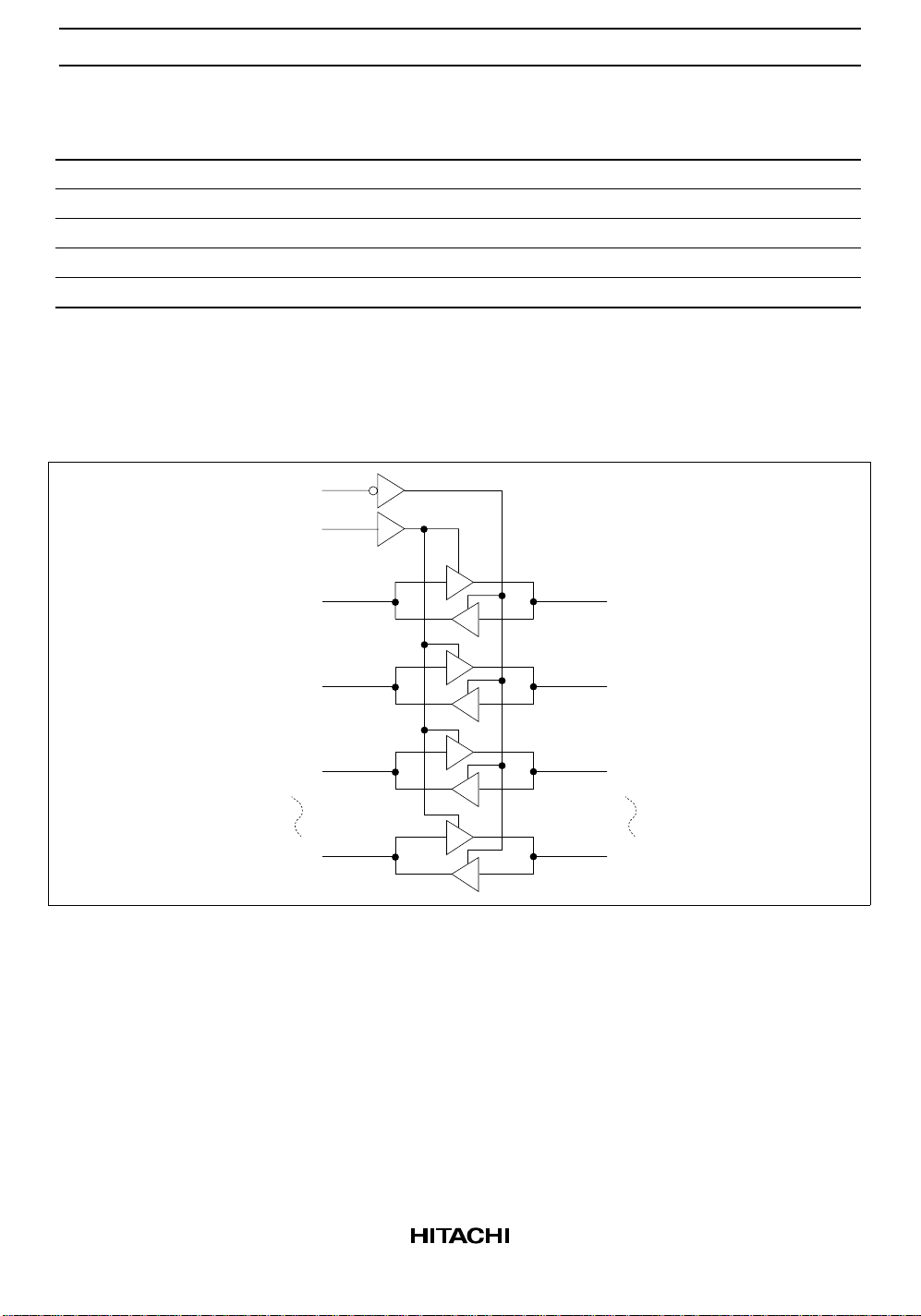
Logic Diagram
GBA
GAB
4.5 5.0 5.5 V
0—VCCV
0—VCCV
0 — 8 ns/V
A1
A2
A3
A8
B1
B2
B3
B8
3
 Loading...