HIT HD74ALVCH162830 Datasheet

HD74ALVCH162830
1-bit to 2-bit Address Driver with 3-state Outputs
ADE-205-197 (Z)
Preliminary
1st. Edition
November 1997
Description
This 1-bit to 2-bit address driver is designed for 2.3 V to 3.6 V VCC operation. To ensure the high
impedance state during power up or power down, OE should be tied to VCC through a pullup resistor; the
minimum value of the resistor is determined by the current sinking capability of the driver. Active bus hold
circuitry is provided to hold unused or floating inputs at a valid logic level. All outputs, which are designed
to sink up to 12 mA, include equivalent 26 Ω resistors to reduce overshoot and undreshoot.
Features
• VCC = 2.3 V to 3.6 V
• Typical VOL ground bounce < 0.8 V (@VCC = 3.3 V, Ta = 25°C)
• Typical VOH undershoot > 2.0 V (@VCC = 3.3 V, Ta = 25°C)
• High output current ±12 mA (@VCC = 3.0 V)
• Bus hold on data inputs eliminates the need for external pullup / pulldown resistors
• All outputs have equivalent 26 Ω series resistors, so no external resistors are required

HD74ALVCH162830
Function Table
Inputs Outputs
OE1 OE2 A 1Yn 2Yn
LHHHZ
LHLLZ
HLHZH
HLLZL
LLHHH
LLLLL
HHXZZ
H : High level
L : Low level
X : Immaterial
Z : High impedance
2

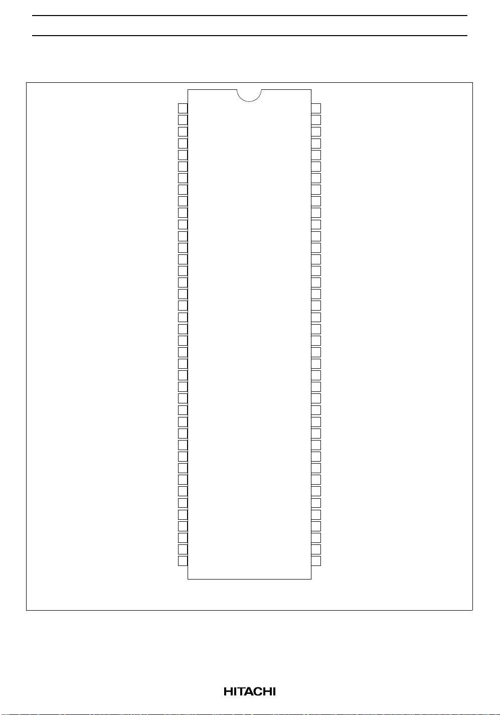
Pin Arrangement
HD74ALVCH162830
V
CC
V
CC
A10
V
CC
V
CC
10A3
11A4
12GND
13A5
14A6
15
16A7
17A8
18GND
19A9
20OE1
21OE2
22
23GND
24A11
25A12
26
27A13
28A14
29GND
30A15
31A16
32GND
33A17
34A18
35
362Y18
371Y18
38GND
392Y17
401Y17
12Y2
21Y2
3GND
42Y1
51Y1
6
7A1
8A2
9GND
80
79
78
77
76
75
74
73
72
71
70
69
68
67
66
65
64
63
62
61
60
59
58
57
56
55
54
53
52
51
50
49
48
47
46
45
44
43
42
41
1Y3
2Y3
GND
1Y4
2Y4
V
CC
1Y5
2Y5
GND
1Y6
2Y6
GND
1Y7
2Y7
V
CC
1Y8
2Y8
GND
1Y9
2Y9
1Y10
2Y10
GND
1Y11
2Y11
V
CC
1Y12
2Y12
GND
1Y13
2Y13
GND
1Y14
2Y14
V
CC
1Y15
2Y15
GND
1Y16
2Y16
(Top view)
3

HD74ALVCH162830
Absolute Maximum Ratings
Item Symbol Ratings Unit Conditions
Supply voltage V
Input voltage
Output voltage
*1
*1, 2
Input clamp current I
Output clamp current I
Continuous output current I
VCC, GND current / pin ICC or I
Maximum power dissipation
at Ta = 55°C (in still air)
*3
Storage temperature T
CC
V
I
V
O
IK
OK
O
GND
P
T
stg
Notes: Stresses beyond those listed under “absolute maximum ratings” may cause permanent damage
to the device. These are stress ratings only, and functional operation of the device at these or
any other conditions beyond those indicated under “recommended operating conditions” is not
implied. Exposure to absolute maximum rated conditions for extended periods may affect device
reliability.
1. The input and output negative voltage ratings may be exceeded if the input and output clamp
current ratings are observed.
2. This value is limited to 4.6 V maximum.
3. The maximum package power dissipation is calculated using a junction temperature of 150°C
and a board trace length of 750 mils.
–0.5 to 4.6 V
–0.5 to 4.6 V
–0.5 to VCC +0.5 V
–50 mA VI < 0
±50 mA VO < 0 or VO > V
±50 mA VO = 0 to V
CC
±100 mA
1 W TVSOP
–65 to 150 °C
CC
Recommended Operating Conditions
Item Symbol Min Max Unit Conditions
Supply voltage V
Input voltage V
Output voltage V
High level output current I
Low level output current I
CC
I
O
OH
OL
Input transition rise or fall rate ∆t / ∆v 0 10 ns / V
Operating temperature T
a
Note: Unused control inputs must be held high or low to prevent them from floating.
2.3 3.6 V
0VCCV
0VCCV
—–6mAV
—–8 V
= 2.3 V
CC
= 2.7 V
CC
— –12 VCC = 3.0 V
— 6 mA VCC = 2.3 V
—8 V
—12 V
= 2.7 V
CC
= 3.0 V
CC
–40 85 °C
4
 Loading...