HIT HD74ALVCH162501 Datasheet

HD74ALVCH162501
18-bit Universal Bus Transceivers with 3-state Outputs
ADE-205-182 (Z)
Preliminary
1st. Edition
December 1996
Description
Data flow in each direction is controlled by output enable (OEAB and OEBA), latch enable (LEAB
and LEBA), and clock (CLKAB and CLKBA) inputs. For A to B data flow, the device operates in the
transparent mode when LEAB is high. When LEAB is low, the A data is latched if CLKAB is held at
a high or low logic level. If LEAB is low, the A bus data is stored in the latch flip flop on the low to
high transition of CLKAB. When OEAB is high, the outputs are active. When OEAB is low, the
outputs are in the high impedance state. Data flow for B to A is similar to that of A to B but uses
OEBA, LEBA, and CLKBA. The output enables are complementary (OEAB is active high, and
OEBA is active low). Active bus hold circuitry is provided to hold unused or floating data inputs at a
valid logic level. All outputs, which are designed to sink up to 12 mA, include 26 Ω resistors to reduce
overshoot and undershoot.
Features
• VCC = 2.3 V to 3.6 V
• Typical VOL ground bounce < 0.8 V (@VCC = 3.3 V, Ta = 25°C)
• Typical VOH undershoot > 2.0 V (@VCC = 3.3 V, Ta = 25°C)
• High output current ±12 mA (@VCC = 3.0 V)
• Bus hold on data inputs eliminates the need for external pullup / pulldown resistors
• All outputs have equivalent 26 Ω series resistors, so no external resistors are required.

HD74ALVCH162501
Function Table
*3
Inputs Output B
OEAB LEAB CLKAB A
LXXXZ
HHXL L
HHXHH
HL↑LL
HL↑HH
HLHXB
HLLXB
*1
0
*2
0
H : High level
L : Low level
X : Immaterial
Z : High impedance
↑ : Low to high transition
Notes: 1. Output level before the indicated steady state input conditions were established, provided
that CLKAB was high before LEAB went low.
2. Output level before the indicated steady state input conditions were established.
3. A to B data flow is show; B to A flow is similar but uses OEBA, LEBA, and CLKBA.

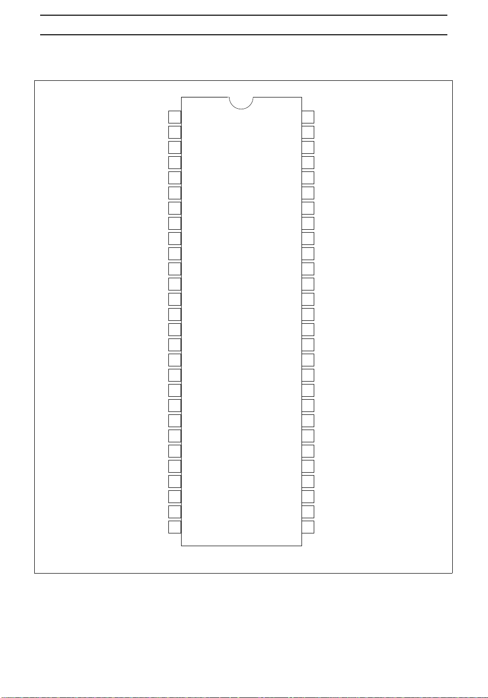
Pin Arrangement
HD74ALVCH162501
OEAB
LEAB
A1
GND
A2
A3
V
CC
A4
A5
A6
GND
A7
A8
A9
A10
A11
A12
GND
A13
A14
A15
V
CC
A16
A17
GND
A18
OEBA
LEBA
10
11
12
13
14
15
16
17
18
19
20
21
22
23
24
25
26
27
28
GND
1
2
3
4
5
6
7
8
9
56
55
54
53
52
51
50
49
48
47
46
45
44
43
42
41
40
39
38
37
36
35
34
33
32
31
30
29
CLKAB
B1
GND
B2
B3
V
CC
B4
B5
B6
GND
B7
B8
B9
B10
B11
B12
GND
B13
B14
B15
V
CC
B16
B17
GND
B18
CLKBA
GND
(Top view)

HD74ALVCH162501
Absolute Maximum Ratings
Item Symbol Ratings Unit Conditions
Supply voltage V
Input voltage
Output voltage
*1, 2
*1, 2
Input clamp current I
Output clamp current I
Continuous output current I
Maximum power dissipation
at Ta = 55°C (in still air)
*3
CC
V
I
V
O
IK
OK
O
P
T
Storage temperature Tstg –65 to 150 °C
Notes: Stresses beyond those listed under “absolute maximum ratings” may cause permanent
damage to the device. These are stress ratings only, and functional operation of the device
at these or any other conditions beyond those indicated under “recommended operating
conditions” is not implied. Exposure to absolute maximum rated conditions for extended
periods may affect device reliability.
1. The input and output negative voltage ratings may be exceeded if the input and output
clamp current ratings are observed.
2. This value is limited to 4.6 V maximum.
3. The maximum package power dissipation is calculated using a junction temperature of
150°C and a board trace length of 750 mils.
–0.5 to 4.6 V
–0.5 to 4.6 V Except I/O ports
–0.5 to VCC +0.5 I/O ports
–0.5 to VCC +0.5 V
–50 mA
±50 mA VO < 0 or VO > V
±50 mA VO = 0 to V
CC
±100
1 W TSSOP
CC
Recommended Operating Conditions
Item Symbol Min Max Unit Conditions
Supply voltage V
Input voltage V
Output voltage V
High level output current I
Low level output current I
CC
I
O
OH
OL
Input transition rise or fall rate ∆t / ∆v 0 10 ns / V
Operating temperature Ta –40 85 °C
Note: Unused control inputs must be held high or low to prevent them from floating.
2.3 3.6 V
0VCCV
0VCCV
—–6mAV
—–8 V
= 2.3 V
CC
= 2.7 V
CC
— –12 VCC = 3.0 V
— 6 mA VCC = 2.3 V
—8 V
—12 V
= 2.7 V
CC
= 3.0 V
CC
 Loading...