HIT HD74ALVCH162270 Datasheet

HD74ALVCH162270
12-bit to 24-bit Registered Bus Exchanger with 3-state Outputs
ADE-205-178A (Z)
2nd. Edition
March 1998
Description
The HD74ALVCH162270 is used in applications where data must be transferred from a narrow high speed
bus to a wide lower frequency bus. The device provides synchronous data exchange between the two ports.
Data is stored in the internal registers on the low to high transition of the clock (CLK) input when the
appropriate CLKEN inputs are low. The select (SEL) line selects 1B or 2B data for the A outputs. For data
transfer in the A to B direction, a two stage pipeline is provided in the A to 1B path, with a single storage
register in the A to 2B path. Proper control of the CLKENA inputs allows two sequential 12-bit words to
be presented synchronously as a 24-bit word on the B port. Data flow is controlled by the active low output
enables (OEA, OEB). The control terminals are registered to synchronize the bus direction changes with
CLK. Active bus hold circuitry is provided to hold unused or floating data inputs at a valid logic level. All
outputs, which are designed to sink up to 12 mA, include 26 Ω resistors to reduce overshoot and
undershoot.
Features
• VCC = 2.3 V to 3.6 V
• Typical VOL ground bounce < 0.8 V (@VCC = 3.3 V, Ta = 25°C)
• Typical VOH undershoot > 2.0 V (@VCC = 3.3 V, Ta = 25°C)
• High output current ±12 mA (@VCC = 3.0 V)
• Bus hold on data inputs eliminates the need for external pullup / pulldown resistors
• All outputs have equivalent 26 Ω series resistors, so no external resistors are required.

HD74ALVCH162270
Function Table
Inputs Outputs
CLK OEA OEB A 1B, 2B
↑ HHZZ
↑H L Z Active
↑ L H Active Z
↑ L L Active Active
Output enable
Inputs Outputs
CLKENA1 CLKENA2 CLK A 1B 2B
XH↑L1B
XH↑H1B
LL↑LL
*1, 2
0
*1, 2
0
*2
LL↑HH *2H
HL↑L1B
HL↑H1B
HHXX1B
*1L
0
*1H
0
*12B0
0
A-to-B storage (OEB = L)
2B0
2B0
L
*1
*1
*1
Note: This functional table describes the case of transferring the same data for A to 1B path. For the case
of transferring different data, see logic diagrams.
2

HD74ALVCH162270
Inputs Output A
CLKEN1B CLKEN2B CLK SEL 1B 2B
HXXHXXA
XHXLXXA
LX↑HL XL
LX↑HHXH
XL ↑LXLL
XL ↑LXHH
B-to-A storage (OEA = L)
H : High level
L : Low level
X : Immaterial
Z : High impedance
↑ : Low to high transition
Notes: 1. Output level before the indicated steady state input conditions were established.
2. Two CLK edges are needed to propagate data.
*1
0
*1
0
3

HD74ALVCH162270
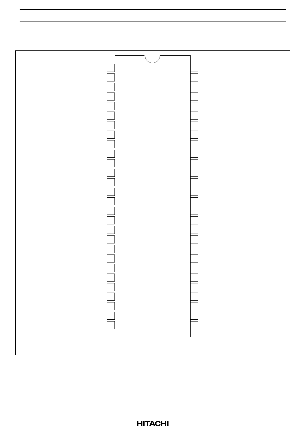
Pin Arrangement
OEA
CLKEN1B
2B3
GND
2B2
2B1
V
CC
A1
A2
A3
GND
A4
A5
A6
A7
A8
A9
GND
A10
A11
A12
V
CC
1B1
1B2
GND
1B3
CLKEN2B
SEL
10
11
12
13
14
15
16
17
18
19
20
21
22
23
24
25
26
27
28
OEB
1
2
3
4
5
6
7
8
9
56
CLKENA2
55
54
2B4
53
GND
2B5
52
51
2B6
50
V
2B7
49
2B8
48
47
2B9
46
GND
2B10
45
2B11
44
43
2B12
42
1B12
1B11
41
1B10
40
GND
39
38
1B9
1B8
37
1B7
36
35
V
34
1B6
33
1B5
32
GND
31
1B4
30
CLKENA1
29
CLK
CC
CC
(Top view)
4

HD74ALVCH162270
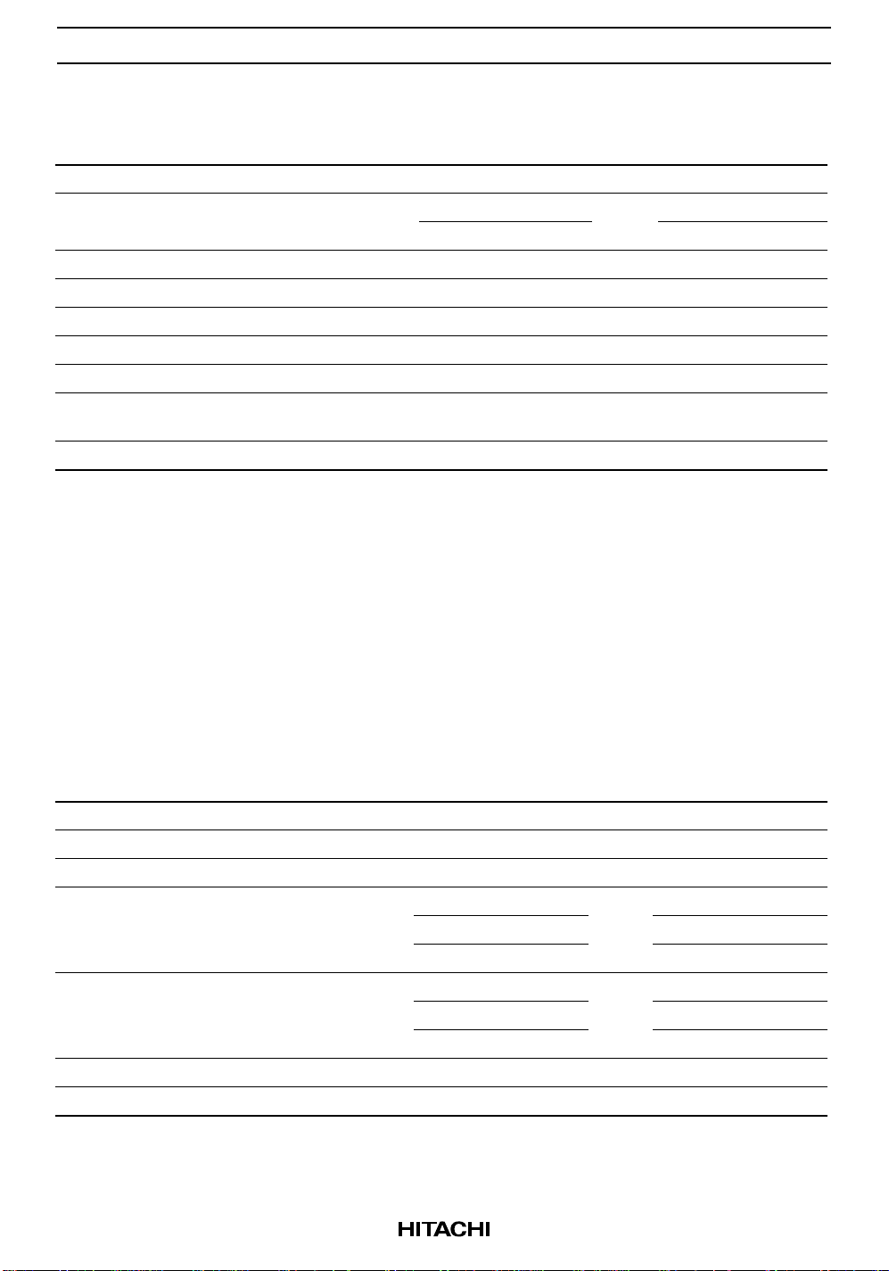
Absolute Maximum Ratings
Item Symbol Ratings Unit Conditions
Supply voltage V
Input voltage
Output voltage
*1, 2
*1, 2
Input clamp current I
Output clamp current I
Continuous output current I
VCC, GND current / pin ICC or I
Maximum power dissipation
at Ta = 55°C (in still air)
*3
CC
V
I
V
O
IK
OK
O
GND
P
T
Storage temperature Tstg –65 to 150 °C
Notes: Stresses beyond those listed under “absolute maximum ratings” may cause permanent damage
to the device. These are stress ratings only, and functional operation of the device at these or
any other conditions beyond those indicated under “recommended operating conditions” is not
implied. Exposure to absolute maximum rated conditions for extended periods may affect device
reliability.
1. The input and output negative voltage ratings may be exceeded if the input and output clamp
current ratings are observed.
2. This value is limited to 4.6 V maximum.
3. The maximum package power dissipation is calculated using a junction temperature of 150°C
and a board trace length of 750 mils.
–0.5 to 4.6 V
–0.5 to 4.6 V Except I/O ports
–0.5 to VCC +0.5 I/O ports
–0.5 to VCC +0.5 V
–50 mA VI < 0
±50 mA VO < 0 or VO > V
±50 mA VO = 0 to V
CC
±100 mA
1 W TSSOP
CC
Recommended Operating Conditions
Item Symbol Min Max Unit Conditions
Supply voltage V
Input voltage V
Output voltage V
High level output current I
Low level output current I
CC
I
O
OH
OL
Input transition rise or fall rate ∆t / ∆v 0 10 ns / V
Operating temperature Ta –40 85 °C
Note: Unused control inputs must be held high or low to prevent them from floating.
2.3 3.6 V
0VCCV
0VCCV
—–6mAV
—–8 V
= 2.3 V
CC
= 2.7 V
CC
— –12 VCC = 3.0 V
— 6 mA VCC = 2.3 V
—8 V
—12 V
= 2.7 V
CC
= 3.0 V
CC
5
 Loading...