HIT HD74ALVC16834 Datasheet

HD74ALVC16834
18-bit Universal Bus Driver with 3-state Outputs
and Inverted Latch Enable
ADE-205-216D (Z)
5th. Edition
December 1999
Description
The HD74ALVC16834 is an 18-bit universal bus driver designed for 2.3 V to 3.6 V VCC operation.
Data flow from A to Y is controlled by output enable (OE). The device operates in the transparent mode
when the latch enable (LE) input is low. The A data is latched if the clock (CLK) input is held at a high or
low logic level. If LE is high, the A data is stored in the latch/flip flop on the low to high transition of the
CLK. When OE is high, the outputs are in the high impedance state.
To ensure the high impedance state during power up or power down, OE should be tied to VCC through a
pullup registor; the minimum value of the registor is determined by the current sinking capability of the
driver.
Features
• Meets “PC SDRAM registered DIMM design support document, Rev. 1.2”
• Typical VOL ground bounce < 0.8 V (@VCC = 3.3 V, Ta = 25°C)
• Typical VOH undershoot > 2.0 V (@VCC = 3.3 V, Ta = 25°C)
• High output current ±24 mA (@VCC = 3.0 V)

HD74ALVC16834
Function Table
Inputs
OE LE CLK A Output Y
HXXXZ
LLXLL
LLXHH
LH↑ LL
LH↑ HH
LHHXY
LHLXY
H : High level
L : Low level
X : Immaterial
Z : High impedance
↑ : Low to high transition
Notes: 1. Output level before the indicated steady-state input conditions were established, provided that
CLK was high before LE went low.
2. Output level before the indicated steady-state input conditions were established.
*1
0
*2
0
2

Pin Arrangement
HD74ALVC16834
NC
NC
Y1
GND
Y2
Y3
V
CC
Y4
Y5
Y6
GND
Y7
Y8
Y9
Y10
Y11
Y12
GND
Y13
Y14
Y15
V
CC
Y16
Y17
GND
Y18
OE
LE
10
11
12
13
14
15
16
17
18
19
20
21
22
23
24
25
26
27
28
56
55
54
53
52
51
50
49
48
47
46
45
44
43
42
41
40
39
38
37
36
35
34
33
32
31
30
29
GND
NC
A1
GND
A2
A3
V
CC
A4
A5
A6
GND
A7
A8
A9
A10
A11
A12
GND
A13
A14
A15
V
CC
A16
A17
GND
A18
CLK
GND
1
2
3
4
5
6
7
8
9
(Top view)
3

HD74ALVC16834
Absolute Maximum Ratings
Item Symbol Ratings Unit Conditions
Supply voltage range V
Input voltage range
Output voltage range
*1
*1, 2
Input clamp current I
Output clamp current I
Continuous output current I
VCC, GND current / pin ICC or I
Maximum power dissipation
at Ta = 55°C (in still air)
*3
CC
V
I
V
O
IK
OK
O
GND
P
T
Storage temperature range Tstg –65 to 150 °C
Stresses beyond those listed under “absolute maximum ratings” may cause permanent damage to the
device. These are stress ratings only, and functional operation of the device at these or any other conditions
beyond those indicated under “recommended operating condition” is not implied. Exposure to absolutemaximum-rated conditions for extended periods may affect device reliability.
Notes: 1. The input and output negative-voltage ratings may be exceeded if the input and output clamp
current ratings are observed.
2. The input and output positive-voltage ratings may be exceeded up to 4.6 V if the input and output
clamp-current ratings are observed.
3. The maximum power dissipation is calculated using a junction temperature of 150°C and board
trace length of 750 mils.
–0.5 to 4.6 V
–0.5 to 4.6 V
–0.5 to VCC+0.5 V
–50 mA VI < 0
±50 mA VO < 0 or VO > V
±50 mA VO = 0 to V
CC
±100 mA
1 W TSSOP
CC
Recommended Operating Conditions
Item Symbol Min Max Unit Conditions
Supply voltage V
Input voltage V
Output voltage V
High-level output current I
Low-level output current I
CC
I
O
OH
OL
Input transition rise or fall rate ∆t/∆v 0 10 ns/V
Operating free-air temperature Ta –40 85 °C
Note: Unused or floating control pins must be held high or low.
2.3 3.6 V
0VCCV
0VCCV
— –12 mA VCC = 2.3 V
— –12 VCC = 2.7 V
— –24 VCC = 3.0 V
—12mAV
—12 V
—24 V
= 2.3 V
CC
= 2.7 V
CC
= 3.0 V
CC
4

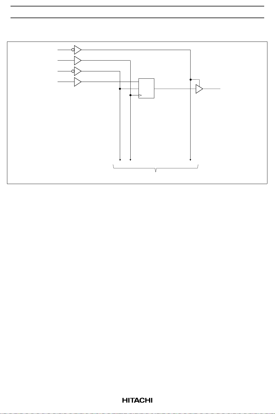
Logic Diagram
OE
CLK
LE
A1
HD74ALVC16834
27
30
28
54
1D
C1
CLK
To seventeen other channels
3
Y1
5
 Loading...