HIT HD74ACT241, HD74AC241 Datasheet

HD74AC241/HD74ACT241
Octal Buffer/Line Driver with 3-State Output
Description
The HD74AC241/HD74ACT241 is an octal buffer and line driver designed to be employed as a memory
address driver, clock driver and bus-oriented transmitter or receiver which provides improved PC board
density.
Features
• 3-State Outputs Drive Bus Lines or Buffer Memory Address Registers
• Outputs Source/Sink 24 mA
• HD74ACT241 has TTL-Compatible Inputs
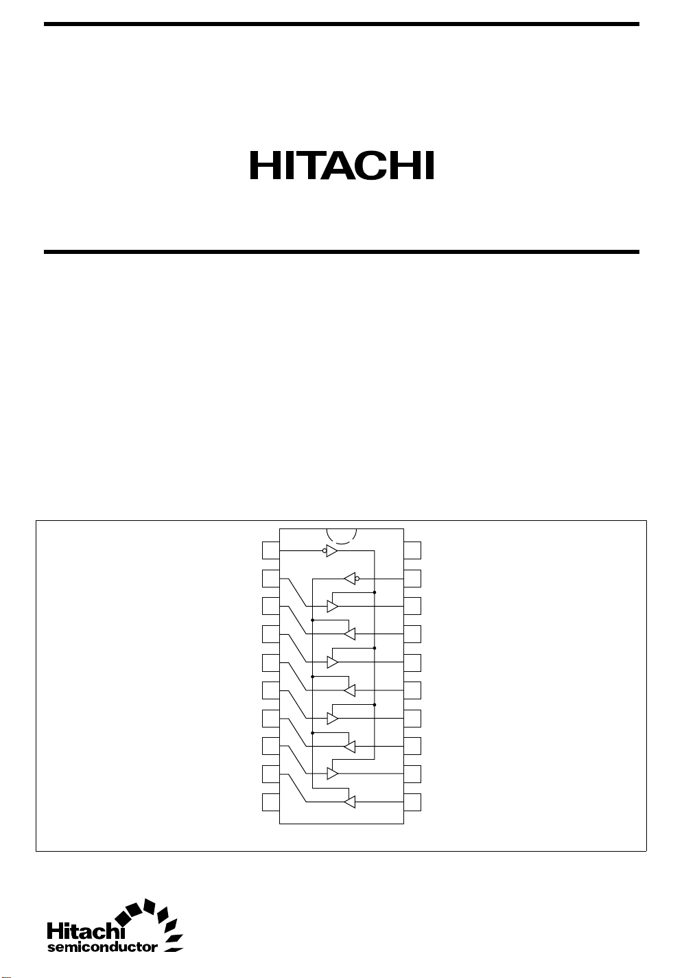
Pin Arrangement
1
OE1V
2
3
4
5
6
7
8
9
10
GND
(Top view)
20
19
18
17
16
15
14
13
12
11
CC
OE2

HD74AC241/HD74ACT241
Truth Tables
Inputs
OE
1
LLL
LHH
HXZ
Inputs
OE
2
HLL
HHH
LXZ
H : High Voltage Level
L : Low Voltage Level
X : Immaterial
Z : High Impedance
D Outputs (Pins 12, 14, 16, 18)
D Outputs (Pins 3, 5, 7, 9)
DC Characteristics (unless otherwise specified)
Item Symbol Max Unit Condition
Maximum quiescent supply current I
Maximum quiescent supply current I
Maximum additional ICC/input
(HD74ACT241)
CC
CC
I
CCT
80 µAV
8.0 µAV
1.5 mA VIN = VCC – 2.1 V, VCC = 5.5 V,
= VCC or ground, VCC = 5.5 V,
IN
Ta = Worst case
= VCC or ground, VCC = 5.5 V,
IN
Ta = 25°C
Ta = Worst case
2

AC Characteristics: HD74AC241
HD74AC241/HD74ACT241
Item Symbol V
Propagation delay t
PLH
Ta = +25°C
C
= 50 pF
L
(V)*1Min Typ Max Min Max Unit
CC
3.3 1.0 6.0 9.0 1.0 10.0 ns
Ta = –40°C to +85°C
CL = 50 pF
Data to output 5.0 1.0 5.0 7.0 1.0 7.5
Propagation delay t
PHL
3.3 1.0 6.0 9.0 1.0 10.5 ns
Data to output 5.0 1.0 4.5 7.0 1.0 7.5
Output enable time t
PZH
3.3 1.0 6.5 12.5 1.0 13.0 ns
5.0 1.0 5.5 9.0 1.0 9.5
Output enable time t
PZL
3.3 1.0 7.0 12.0 1.0 13.0 ns
5.0 1.0 5.5 9.0 1.0 9.5
Output disable time t
PHZ
3.3 1.0 8.0 12.0 1.0 12.5 ns
5.0 1.0 6.5 10.0 1.0 10.5
Output disable time t
PLZ
3.3 1.0 7.0 12.5 1.0 13.5 ns
5.0 1.0 6.0 10.0 1.0 10.5
Note: 1. Voltage Range 3.3 is 3.3 V ± 0.3 V
Voltage Range 5.0 is 5.0 V ± 0.5 V
AC Characteristics: HD74ACT241
Item Symbol V
Propagation delay
t
PLH
(V)*1Min Typ Max Min Max Unit
CC
5.0 1.0 6.5 9.0 1.0 10.0 ns
Data to output
Propagation delay
t
PHL
5.0 1.0 7.0 9.0 1.0 10.0 ns
Data to output
Output enable time t
Output enable time t
Output disable time t
Output disable time t
PZH
PZL
PHZ
PLZ
5.0 1.0 6.0 9.0 1.0 10.0 ns
5.0 1.0 7.0 10.0 1.0 11.0 ns
5.0 1.0 8.0 10.5 1.0 11.5 ns
5.0 1.0 7.0 10.5 1.0 11.5 ns
Note: 1. Voltage Range 5.0 is 5.0 V ± 0.5 V
Ta = +25°C
C
= 50 pF
L
Ta = –40°C to +85°C
CL = 50 pF
3
 Loading...