HIT HD74ACT165, HD74AC165 Datasheet

HD74AC165/HD74ACT165
Parallel-Load 8-bit Shift Register
Description
This 8-bit serial shift register shifts data from QA to QH when clocked, Parallel inputs to each stage are
enabled by a low level at the Shift/Load Input. Also included is a gated clock input and a complementary
output from the eighth bit.
Clocking is accomplished through a 2-input NOR gate permitting one input to be used as a clock inhibit
function. Holding either of the clock inputs high inhibits clocking, and holding either clock input low with
the Shift/Load input high enables the other clock input. Data transfer occurs on the positive going edge of
the clock. Parallel loading is inhibited as long as the Shift/Load input is high. When taken low, data at the
parallel inputs is loaded directly into the register independent of the state of the clock.
Features
• Outputs Source/Sink 24 mA
• HD74ACT165 has TTL-Compatible Inputs

HD74AC165/HD74ACT165
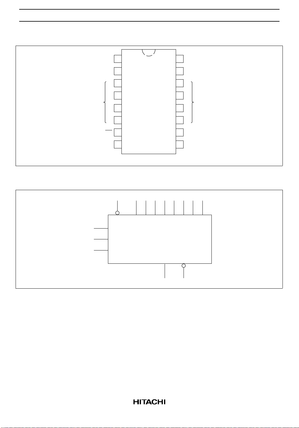
Pin Arrangement
L
S
CP
1
2
16
15
V
CC
Clock
Inhibit
Logic Symbol
Parallel
Inputs
1
2
10
3
E
4
F
5
G
H
6
H
Q
7
89
GND
(Top view)
15 11 12 13 14 3 4
Clock
Inhibit
S
L
CP
SI
A
BCDEFGH
14
13
12
11
10
H QH
Q
D
C
B
A
SI
QH
56
Parallel
Inputs
Pin Names
A to H Parallel Inputs
S
I
CP Clock Input
S
L
Clock Inhibit Clock Inhibit
QH, Q
H
2
Serial Input
Shift Load
Outputs
97

HD74AC165/HD74ACT165
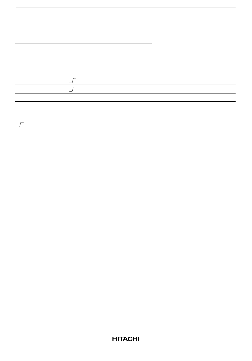
Truth Table
Inputs
Clock Parallel Internal Outputs Outputs
S
L
L X X X a ······ h a b h
HLLXXQ
HL HXHQAnQ
HL LXLQAnQ
HHXXXQ
H : High Voltage Level
L : Low Voltage Level
X : Immaterial
: Low-to-High Clock Transition
Inhibit CP S
I
A ······ H Q
A
AD
AD
Q
B
Q
BO
Q
BO
Q
H
Q
HO
Gn
Cn
Q
HO
3

HD74AC165/HD74ACT165
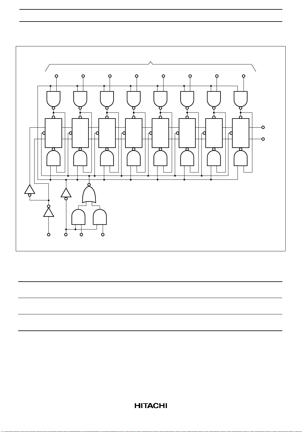
Logic Diagram
Parallel
Inputs
A
Preset
Q
A
S
Clock
QA
R
Clear
SI SL CP Clock
Preset
S
Clock
R
Clear
B
Preset
Q
B
S
Clock
QB
R
Clear
Inhibit
C
Q
C
QC
Preset
S
Clock
R
Clear
D
Q
D
QD
Preset
S
Clock
R
Clear
E
Q
E
QE
Preset
S
Clock
R
Clear
F
Q
F
QF
Preset
S
Clock
R
Clear
G
Q
G
QG
Preset
S
Clock
R
Clear
H
Q
QH
H
Output
H
Q
Output
H
Q
DC Characteristics (unless otherwise specified)
Item Symbol Max Unit Condition
Maximum quiescent supply current I
Maximum quiescent supply current I
Maximum additional ICC/input
(HD74ACT165)
4
CC
CC
I
CCT
80 µAV
8.0 µAV
1.5 mA VIN = VCC – 2.1 V, VCC = 5.5 V,
= VCC or ground, VCC = 5.5 V,
IN
Ta = Worst case
= VCC or ground, VCC = 5.5 V,
IN
Ta = 25°C
Ta = Worst case
 Loading...