HIT HD74ACT112, HD74AC112 Datasheet

HD74AC112/HD74ACT112
Dual JK Negative Edge-Triggered Flip-Flop
Description
The HD74AC112/HD74ACT112 features individual J, K, Clock and asynchronous Set and Clear inputs to
each flip-flop. When the clock goes High, the inputs are enabled and data will be accepted. The logic level
of the J and K inputs may change when the clock is High and the bistable will perform according to the
Truth Table as long as minimum setup and hold times are observed. Input data is transferred to the outputs
on the falling edge of the clock pulse.
Features
• Outputs Source/Sink 24 mA
• HD74ACT112 has TTL-Compatible Inputs
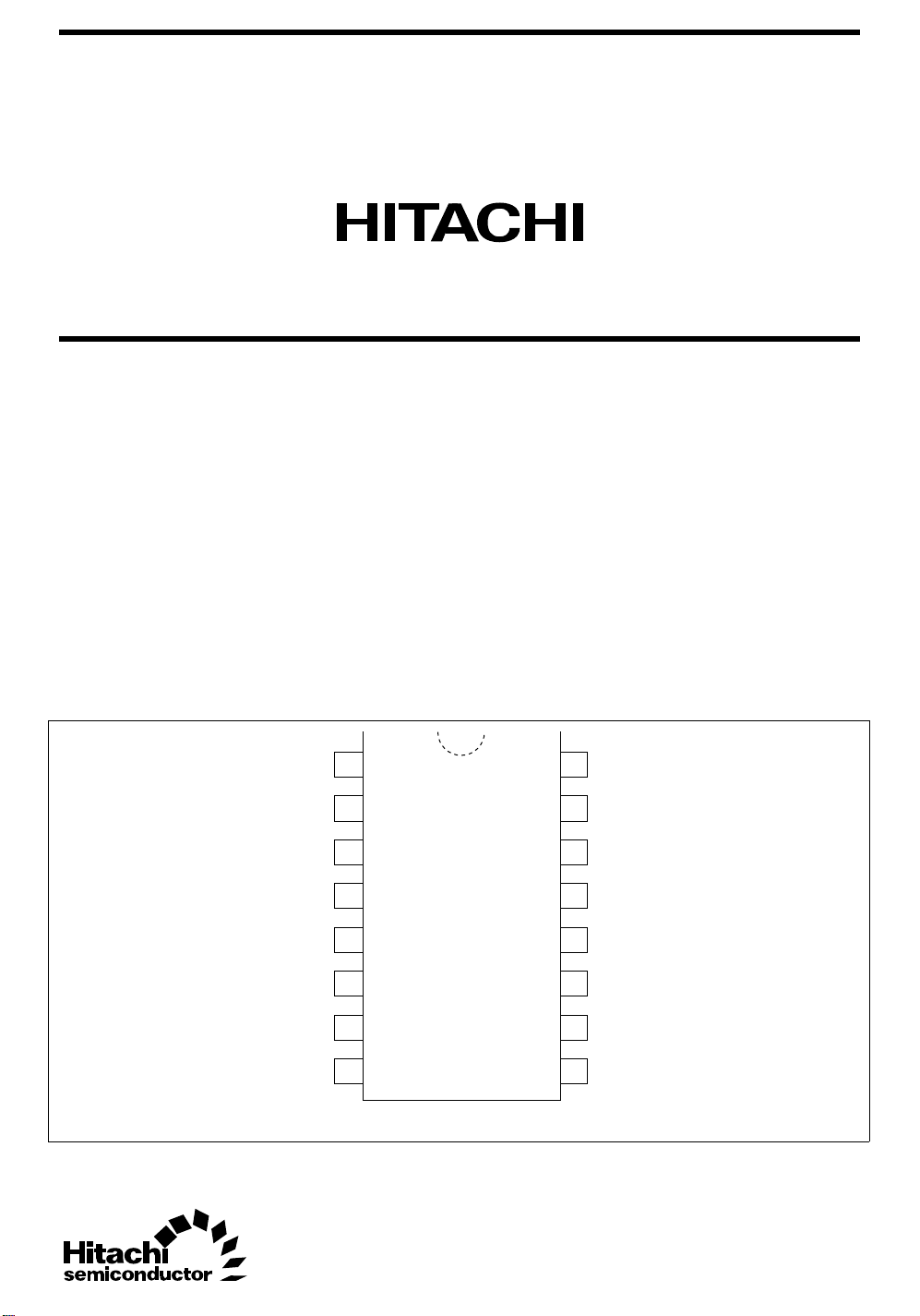
Pin Arrangement
CP
K
J
S
D1
Q
Q
Q
GND
1
1
2
1
3
1
4
5
1
6
1
7
2
8
(Top view)
16
15
14
13
12
11
10
V
CC
C
D1
C
D2
CP
2
K
2
J
2
S
D2
9
Q
2

HD74AC112/HD74ACT112
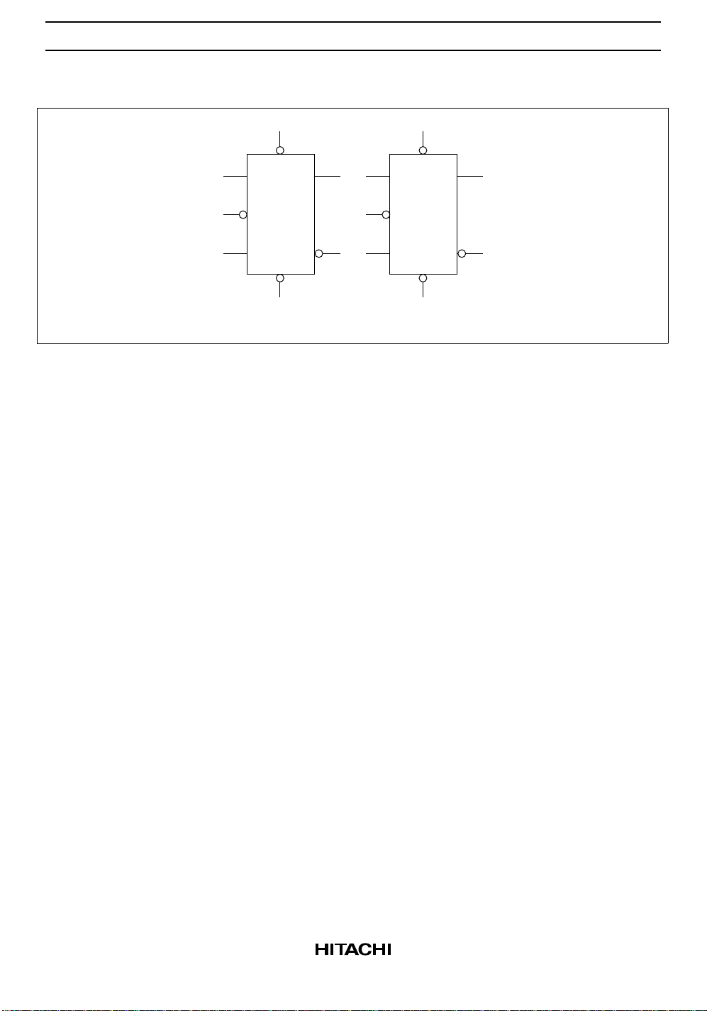
Logic Symbol
410
S
3
1
2
D1
J
1
CP
K
Q
1
Q
1
C
D1
15 14
1
1
V
CC
5
13
6
= Pin16
GND = Pin8
Pin Names
J1, J2, K1, K
CP1, CP
CD1, C
SD1, S
2
D2
D2
Q1, Q2, Q1, Q 2Outputs
Asynchronous Inputs:
Low input to SD sets Q to High level
Low input to CD sets Q to Low level
Clear and Set are independent of clock
Simultaneous Low on CD and SD makes both Q and Q High
Data Inputs
2
Clock Pulse Inputs (Active Falling Edge)
Direct Clear Inputs (Active Low)
Direct Set Inputs (Active Low)
11
12
J
2
CP
K
S
D2
Q
2
Q
2
C
D2
9
2
7
2
2

HD74AC112/HD74ACT112
Truth Table
Inputs Outputs
@t
n
JK Q
LL Qn
LH L
HL H
HH Qn
t
: Bit time before clock pulse.
n
t
: Bit time after clock pulse.
n + 1
H : High Voltage Level
L : Low Voltage Level
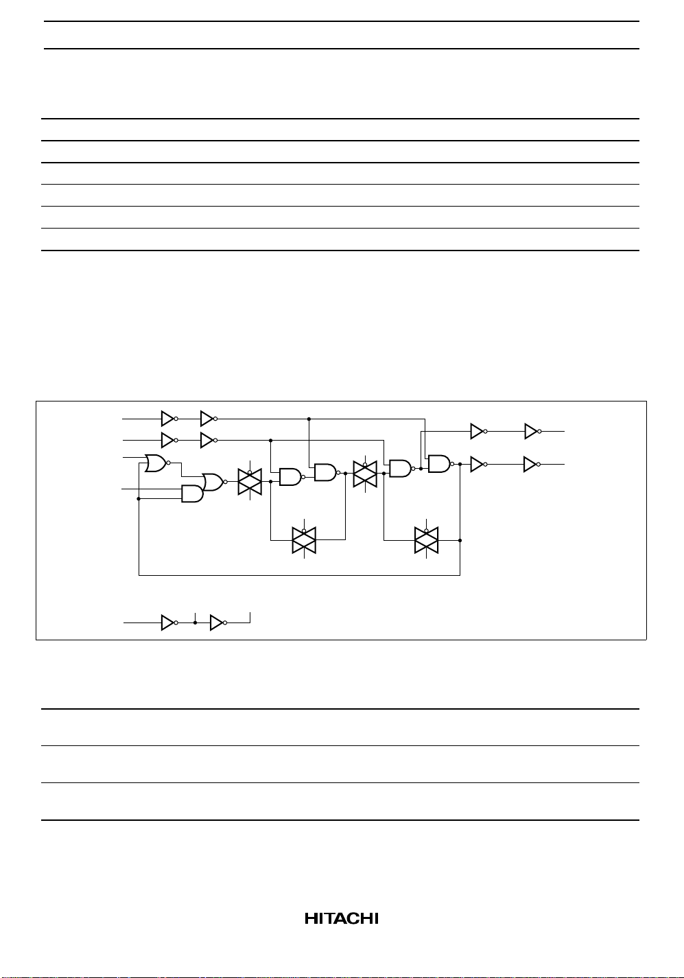
Logic Diagram
S
D
C
D
J
CP
#CP
@t
n + 1
Q
Q
K
#
CP
CP
CP
#
CP
CP
CP
CP
#
#
CP
CP
DC Characteristics (unless otherwise specified)
Item Symbol Max Unit Condition
Maximum quiescent supply current I
Maximum quiescent supply current I
Maximum additional ICC/input
(HD74ACT112)
CC
CC
I
CCT
80 µAV
8.0 µAV
1.5 mA VIN = VCC – 2.1 V, VCC = 5.5 V
= VCC or ground, VCC = 5.5 V,
IN
Ta = Worst case
= VCC or ground, VCC = 5.5 V,
IN
Ta = 25°C
Ta = Worst case
3
 Loading...