HIT HD74AC4024 Datasheet

HD74AC4024
7-State Binary Counter
Description
The HD74AC4024 is a 4-stage counter. This device is incremented on the falling edge (negative transition)
of the input clock, and all its output is reset to a low level by applying a logical high on its reset input.
Feature
• Outputs Source/Sink 24 mA
Pin Arrangement
Q
Q6
Q5
Q4
GND
1
2
7
3
4
5
6
7
(Top view)
14
13
12
11
10
9
8
Clock V
Reset
NC
Q
Q2
NC
Q3
NC
CC
1

HD74AC4024
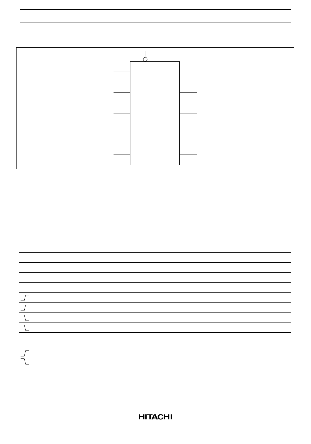
Logic Symbol
C
R
7
Q
Q6
Q5
Q4 Q3
Q1
Q2
Pin Names
Clock Clock Input (Active Falling Edge)
Reset Master Reset Input
Q1 to Q
7
Outputs
Function Table
Clock Reset Outputs State
L L No change
L H All outputs are low
H L No change
H H All outputs are low
L No change
H All outputs are low
L Advance to next state
H All outputs are low
H : High voltage level
L : Low voltage level
: Low-to-High Clock Transition
: High-to-Low Clock Transition
2

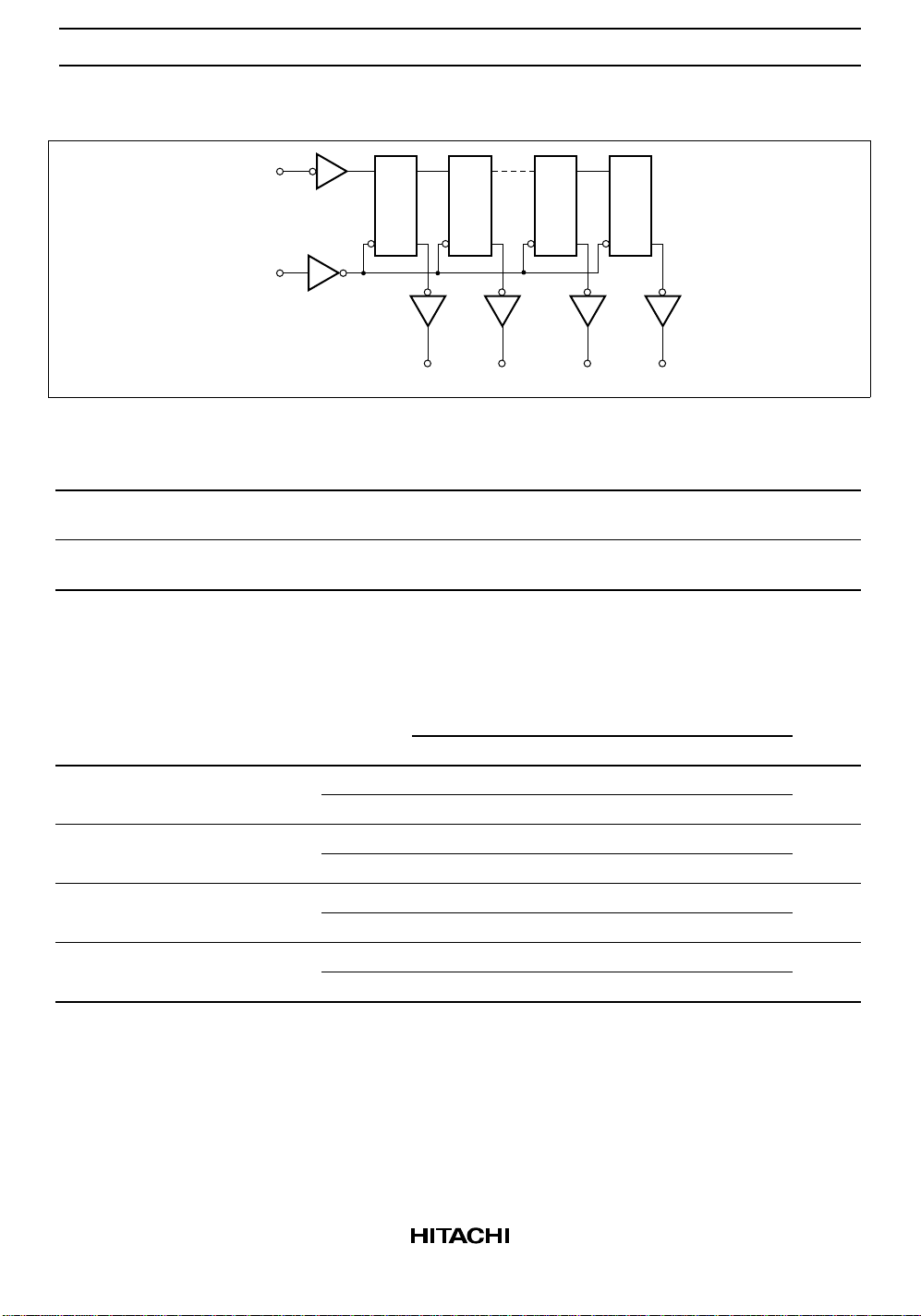
Logic Diagram
HD74AC4024
Clock
Reset
CQ
R
CQ
Q R
Q1 Q2 Q3 Q4
Q R
CQ
Q R
CQ
Q
DC Characteristics (unless otherwise specified)
Item Symbol Max Unit Condition
Maximum quiescent supply current I
CC
80 µAV
= VCC or ground, VCC = 5.5 V,
IN
Ta = Worst case
Maximum quiescent supply current I
CC
8.0 µAV
= VCC or ground, VCC = 5.5 V,
IN
Ta = 25°C
AC Characteristics
Ta = +25°C
C
= 50 pF
L
Item Symbol V
Maximum clock f
max
(V)*1Min Typ Max Min Max Unit
CC
3.3 70 — — 60 — MHz
frequency 5.0 110 — — 95 —
Propagation delay t
Clock to Q
1
Propagation delay t
Clock to Q
1
Propagation delay t
PLH
PHL
PHL
3.3 1.0 9.5 12.5 1.0 13.5 ns
5.0 1.0 7.0 9.0 1.0 9.5
3.3 1.0 9.5 12.0 1.0 13.0 ns
5.0 1.0 6.5 9.0 1.0 10.0
3.3 1.0 10.5 12.5 1.0 13.5 ns
Reset to outputs 5.0 1.0 7.5 10.0 1.0 11.0
Note: 1. Voltage Range 3.3 is 3.3 V ± 0.3 V
Voltage Range 5.0 is 5.0 V ± 0.5 V
Ta = –40°C to +85°C
CL = 50 pF
3
 Loading...