

HIT HD74AC393 Datasheet
HD74AC393
Dual Modulo-16-Counter
Description
The HD74AC393 contains a pair of high speed 4-stage ripple counters. Each half of the HD74AC393
operates as a modulo-16 binary divider, with the last three stages triggered in a ripple fashion. The flipflops are triggered by a High-to-Low transition of their CP inputs. Each half of each circuit type has a
Master Reset input which responds to a High signal by forcing all four outputs to the Low state.
Feature
• Outputs Source/Sink 24 mA
Pin Arrangement
CP
MR
Q
Q1
Q2
Q3
GND
1
2
0
3
4
5
6
7
(Top view)
14
13
12
11
10
CC
V
CP
MR
0
Q
Q1
Q2
9
Q3
8
HD74AC393
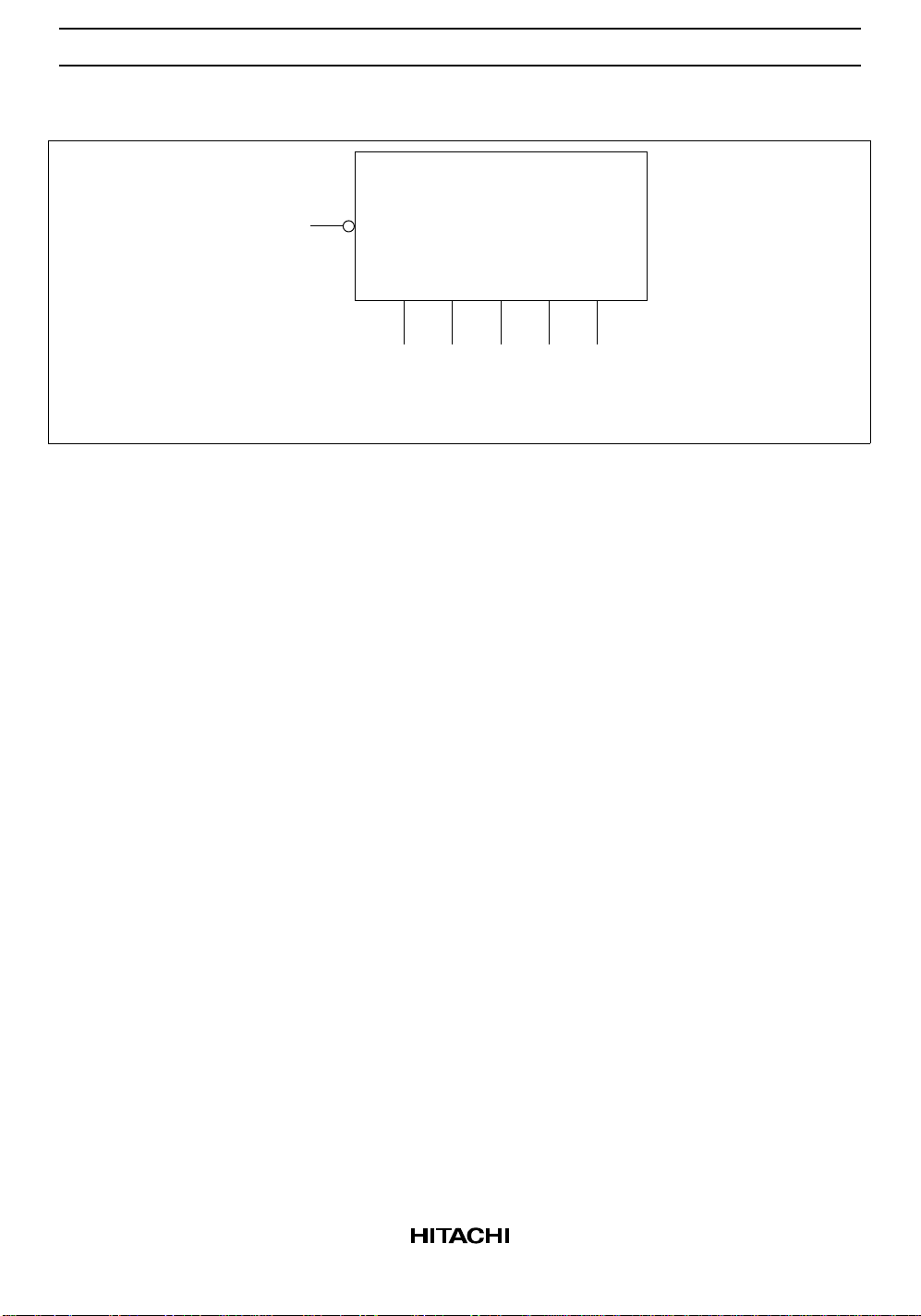
Logic Symbol (each half)
1, 13
CP
MR Q0 Q1 Q2 Q3
2, 12
4, 10 6, 8
3, 11 5, 9
Vcc=Pin14
GND=Pin7
Pin Names
CP Clock Pulse Input (Active Falling Edge)
MR Asynchronous Master Reset Input (Active High)
Q0 – Q3Flip-flop Outputs
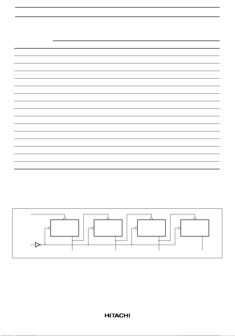
Functional Description
Each half of the HD74AC393 operates in the modulo-16 binary sequence, as indicated in the + 16 Truth
Table. The first flip-flop is triggered by High-to-Low transitions of the CP input signal. Each of the other
flip-flops is triggered by a High-to-Low transition of the Q output of the preceding flip-flop. Thus state
changes of the Q outputs do not occur simultaneously. This means that logic signals derived from
combinations of these outputs will be subject to decoding spikes and, therefore, should not be used as
clocks for other counters, registers or flip-flops. A High signal on MR forces all outputs to the Low state
and prevents counting.
2
HD74AC393
Truth Table
Outputs
Count Q
3
Q
2
0L L L L
1L L L H
2L L H L
3L L H H
4L H L L
5L H L H
6L H H L
7L H H H
8H L L L
9H L L H
10HL HL
11HL HH
12 H H L L
13 H H L H
14HHHL
15HHHH
H : High Voltage Level
L : Low Voltage Level
Q
1
Q
0
Logic Diagram (one, half shown)
CP
K
CP J
D
C
Q
MR
Q
0 Q1 Q2 Q3
K
K
K
CP J
D
C
Q
CP J
D
C
Q
CP J
D
C
Q
3
 Loading...