HIT HD74AC259 Datasheet

HD74AC259
8-bit Addressable Latch
Description
The HD74AC259 is a high-speed 8-bit addressable latch designed for general purpose storage applications
in digital systems. It is a multifunctional device capable or storing single line data in eight addressable
latches, and also a 1-of-8 decoder and demultiplexer with active HIGH outputs. The device also
incorporates an active LOW Common Clear for resetting all latches, as well as an active LOW Enable.
Features
• Serial-to-Parallel Conversion
• Eight Bits of Storage with Output of Each Bit Available
• Random (Addressable) Data Entry
• Active High Demultiplexing or Decoding Capability
• Easily Expandable
• Common Clear
• Outputs Source/Sink 24 mA

HD74AC259
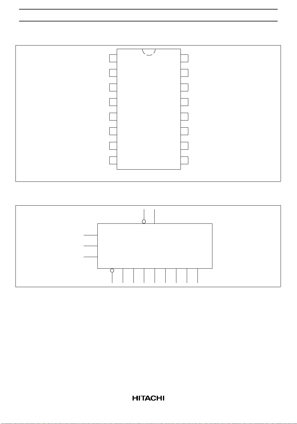
Pin Arrangement
Logic Symbol
A
A1
A2
Q0
Q1
Q2
Q3
GND
A0
1
0
2
3
4
5
6
7
8
(Top view)
ED
16
15
14
13
12
11
10
CC
V
MR
E
D
7
Q
Q6
Q5
9
Q4
A1
A2
Pin Names
A0 – A2Address Inputs
D Data Inputs
E Enable Input (Active LOW)
MR Master Reset (Active LOW)
Q0 – Q7Latch Outputs
2
MR Q0 Q1 Q2
Q
3Q4Q5Q6Q7

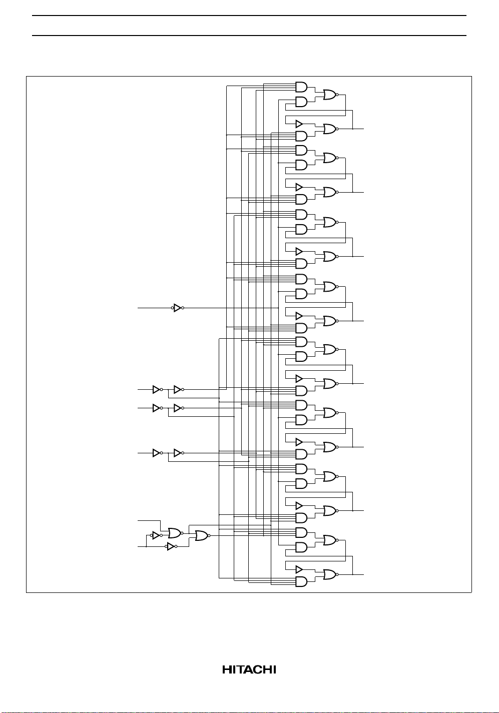
Logic Diagram
HD74AC259
Q7
Q6
Q5
MR
Q4
A
2
A1
A0
D
E
Q3
Q2
Q1
Q0
3

HD74AC259
Function Table
Inputs Outputs
Operating Mode MR E DA
Master reset L H X XXXLLLLLLLL
Demultiplex L L d LLLQ = dLLLLLLL
(Active HIGH L L d H L L L Q = d LLLLLL
Decoder when L L d L H L L L Q = d LLLLL
D = H) LLdHHLLLLQ = dLLLL
LLdLLHLLLLQ = dLLL
LLdHLHLLLLLQ = dLL
LLdLHHLLLLLLQ = dL
LLdHHHLLLLLLLQ = d
Store (Do nothing) H H X XXXq0q1q2q3q4q5q6q
Addressable latch H L d LLLQ = dq1q2q3q4q5q6q
HLdHLLq0Q = d q
HLd LHLq0q1Q = d q
HLd HHLq0q1q2Q = d q
HLdLLHq0q1q2q3Q = d q
HLd HLHq0q1q2q3q4Q = d q
HLd LHHq0q1q2q3q4q5Q = d q
HLd HHHq0q1q2q3q4q5q6Q = d
H : High Voltage Level
L : Low Voltage Level
X : Immaterial
d : High or Low data one setup time prior to the Low-to-High Enable transition.
q : Lower case letters indicate the state of the referenced output established during the last cycle in
which it was addressed or cleared.
A1A2Q0Q1Q2Q3Q4Q5Q6Q
0
q
q
q
2
3
4
q
3
4
4
q
5
6
q
q
5
6
q
q
5
6
q
5
6
6
7
7
7
q
7
q
7
q
7
q
7
q
7
7
DC Characteristics (unless otherwise specified)
Item Symbol Max Unit Condition
Maximum quiescent supply current I
Maximum quiescent supply current I
4
CC
CC
80 µAV
8.0 µAV
= VCC or ground, VCC = 5.5 V,
IN
Ta = Worst case
= VCC or ground, VCC = 5.5 V,
IN
Ta = 25°C
 Loading...