

HIT HD74AC195 Datasheet

HD74AC195
4-bit Parallel-Access Shift Register
Description
This shift register features parallel inputs, parallel outputs, J-K serial inputs, Shift/Load control input, and a
direct overriding clear. This shift register can operate in two modes: Parallel load; Shift from Q0 towards
Q3.
Parallel loading is accomplished by applying the four bits of data, and taking the PE Input low. The data is
loaded into the associated flip-flops and appears at the outputs after the positive transition of the CP input.
During parallel loading, serial data flow is inhibited. Serial shifting occurs synchronously when the PE
input is high. Serial data for this mode is entered at the J-K inputs. These inputs allow the first stage to
perform as a J-K or toggle flip-flop as shown in the function table.
Features
• Shift Right and Parallel Load Capability
• J-K (D-Type) Inputs to First Stage
• Complement Output from Last Stage
• Asynchronous Master Reset
• Outputs Source/Sink 24 mA
HD74AC195
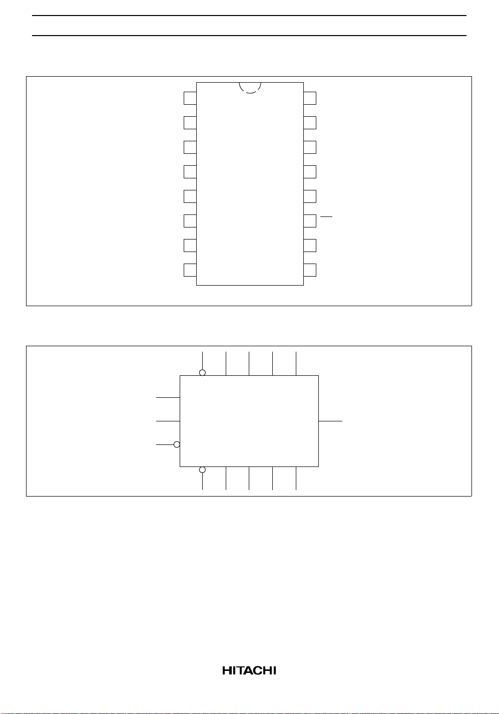
Pin Arrangement
Logic Symbol
MR
D
D1
D2
D3
GND
J
K
0
1
2
3
4
5
6
7
8
J
PE D
(Top view)
0 D1 D2 D3
16
15
14
13
12
11
10
CC
V
Q0
Q1
Q2
Q3
Q3
CP
9
PE
CP
K
MR Q0 Q1 Q2 Q3
Pin Names
CP Clock Pulse Input (Active Rising Edge)
D0 to D
3
PE Parallel Enable Input
MR Asynchronous Master Reset
J, K J-K or D Type Serial Inputs
Q0 to Q3, Q
2
Parallel Data Inputs
Outputs
3
3
Q
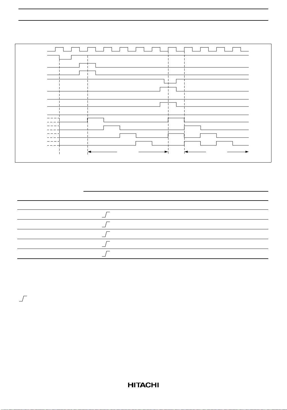
Timing Diagram
CP
MR
J
K
PE
HD74AC195
D
D1
D2
D3
Q0
Q1
Q2
Q3
0
Serial Shift Serial Shift
H
L
H
L
LoadClear
Mode Select-Function Table
Inputs Outputs
Q
Q
Q
Q
Operating Modes MR CP PE J K D
n
0
1
2
Asynchronous Reset L X XXXXLLL LH
Shift, Set First Stage H HHHXHq0q1q
Shift, Reset First Stage H HLLXLq0q1q
Shift, Toggle First Stage H HHLXq0q0q1q
Shift, Retain First Stage H HLHXq0q0q1q
Parallel Load H LXXdnd0d1d2d
H : HIGH Voltage Level
L : LOW Voltage Level
X : Immaterial
Lower case letters indicate the state of the referenced input (or output) one setup time prior to the LOW-to-
HIGH transition.
: LOW-to-HIGH clock transition.
3
2
2
2
2
3
Q
3
q
2
q
2
q
2
q
2
d
3
3
HD74AC195
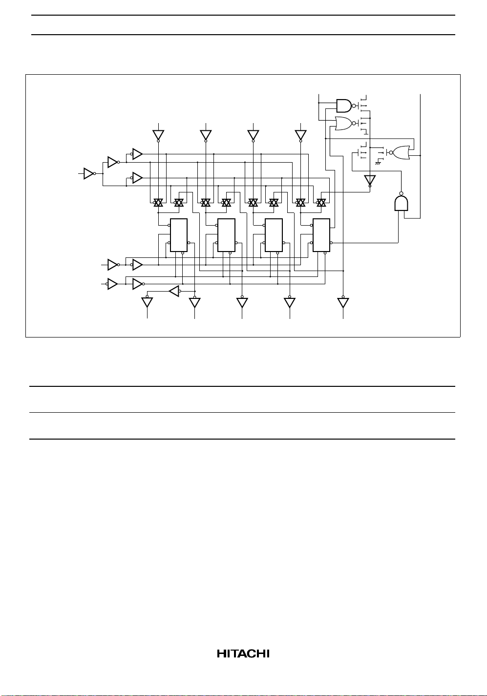
Logic Diagram
D
3 D2 D1 D0
PE
CP
MR
DC Characteristics (unless otherwise specified)
K
VCC J
V
CC
Q0Q1Q2Q3Q3
Item Symbol Max Unit Condition
Maximum quiescent supply current I
CC
80 µAV
= VCC or ground, VCC = 5.5 V,
IN
Ta = Worst case
Maximum quiescent supply current I
CC
8.0 µAV
= VCC or ground, VCC = 5.5 V,
IN
Ta = 25°C
4
 Loading...