

HIT HD74AC166 Datasheet
HD74AC166/HD74ACT166
8-bit Shift Register
Description
The HD74AC166/HD74ACT166 is an 8-bit, serial or parallel-in, serial-out shift register using edge
triggered D-type flip-flops. Serial and parallel entry are synchronous, with state changes initiated by the
rising edge of the clock. An asynchronous Master Reset overrides other inputs and clears all flip-flops.
The circuit can be clocked from two sources or one CP input can be used to trigger the other.
Features
• Outputs Source/Sink 24 mA
• HD74ACT166 has TTL-Compatible Inputs
Pin Arrangement
D
P0
P1
P2
P3
CP2
CP1
GND
1
S
2
3
4
5
6
7
8
(Top view)
16
15
14
13
12
11
10
CC
V
PE
7
P
Q7
P6
P5
P4
9
MR
HD74AC166/HD74ACT166
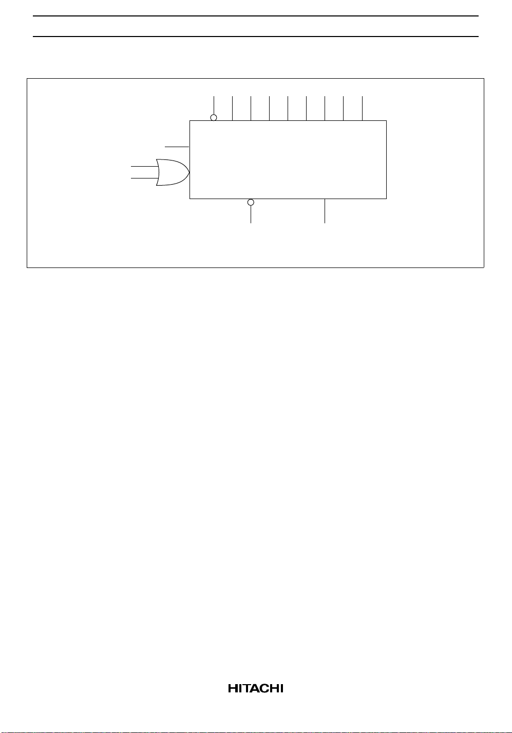
Logic Symbol
15
2 3 4 5 10 11 12 14
P
0
PE P
1 P2 P3 P4 P5 P6 P7
1
71
6
2
DS
CP
MR
913
V
CC=Pin16
GND=Pin8
7
Q
Pin Names
CP1, CP2Clock Pulse Inputs (Active Rising Edge)
D
S
Serial Data Input
PE Parallel Enable Input (Active Low)
P0 to P
Parallel Data Inputs
7
MR Asynchronous Master Reset Input (Active Low)
Q
7
Last Stage Output
Functional Description
Operation is synchronous (except for Master Reset) and state changes are initiated by the rising edge of
either clock input if the other clock input is Low. When one of the clock inputs is used as an active High
clock inhibt, it should attain the High state while the other clock is still in the High state following the
previous operation. When the Parallel Enable (PE) input is Low, data is loaded into the register from the
Parallel Data (P0 to P7) inputs on the next rising edge of the clock. When PE is High, information is shifted
from the Serial Data (DS) input to Q0 and all data in the register is shifted one bit position (i.e., Q0 → Q1, Q
→ Q2, etc.) on the rising edge of the clock.
1
2
HD74AC166/HD74ACT166
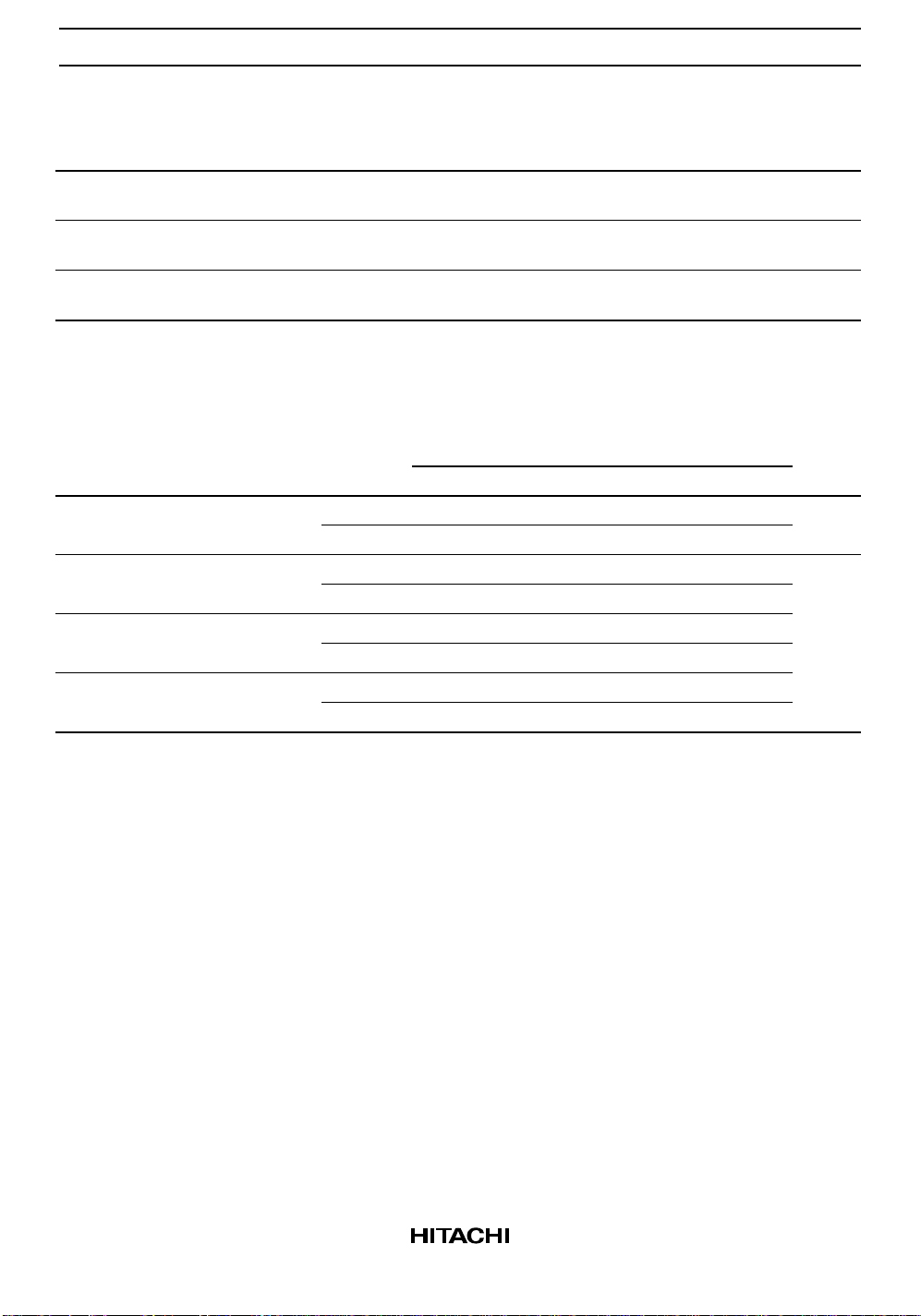
Truth Table
Inputs
Parallel Internal Outputs Output
MR PE CP
2
LXXXXXL LL
HXLLXXQA0Q
HL L X a ··· h a b h
HH L HXHQAnQ
HH L LXLQAnQ
HX H XXQA0Q
H : High Voltage Level
L : Low Voltage Level
X : Immaterial
: Low-to-High Clock Transition
Logic Diagram
CP
1
D
S
P0 to P
Q
7
0
Q
6
B0
B0
Q
7
Q
H0
Gn
Gn
Q
H0
P
0 P1 P2 P3 P4 P5 P6 P7
RCP
C
D
S
S
Q
MR PED
RCPS
C
D
Q
Q
CP
12
7
3
HD74AC166/HD74ACT166
DC Characteristics (unless otherwise specified)
Item Symbol Max Unit Condition
Maximum quiescent supply current I
Maximum quiescent supply current I
Maximum additional ICC/input
CC
CC
I
CCT
(HD74ACT166)
AC Characteristics: HD74AC166
80 µAV
8.0 µAV
1.5 mA VIN = VCC – 2.1 V, VCC = 5.5 V,
= VCC or ground, VCC = 5.5 V,
IN
Ta = Worst case
= VCC or ground, VCC = 5.5 V,
IN
Ta = 25°C
Ta = Worst case
Item Symbol V
Maximum clock f
max
Ta = +25°C
C
= 50 pF
L
(V)*1Min Typ Max Min Max Unit
CC
3.3 75 — — 65 — MHz
Ta = –40°C to +85°C
CL = 50 pF
frequency 5.0 100 — — 80 —
Propagation delay t
CP1 or CP2 to Q
7
Propagation delay t
CP1 or CP2 to Q
7
Propagation delay t
MR to Q
7
PLH
PHL
PHL
3.3 1.0 11.0 14.5 1.0 15.5 ns
5.0 1.0 9.5 11.5 1.0 12.5
3.3 1.0 10.5 14.0 1.0 15.0
5.0 1.0 9.0 11.0 1.0 12.0
3.3 1.0 9.5 12.0 1.0 13.0
5.0 1.0 6.5 9.0 1.0 10.0
Note: 1. Voltage Range 3.3 is 3.3 V ± 0.3 V
Voltage Range 5.0 is 5.0 V ± 0.5 V
4
 Loading...