HIT HD74AC158 Datasheet

HD74AC158
Quad 2-Input Multiplexer
Description
The HD74AC158 is a high-speed quad 2-input multiplexer. It selects four bits of data from two source
using the common Select and Enable inputs. The four buffered outputs present the selected data in the
inverted form. The HD74AC158 can also be used as a function generator.
Feature
• Outputs Source/Sink 24 mA
Pin Arrangement
I
I1a
Za
I0b
I1b
Zb
GND
1
S
0a
2
3
4
5
6
7
8
(Top view)
16
15
14
13
12
11
10
CC
V
E
0c
I
I1c
Zc
I0d
I1d
9
Zd

HD74AC158
Logic Symbol
Pin Names
I0a to I0dSource 0 Data Inputs
I1a to I1dSource 1 Data Inputs
E Enable Input
S Select Input
Za to ZdOutputs
S
EI
0a
I1a I0b I0c I1c Iod I1dI1b
Za Zb Zc Zd
Functional Description
The HD74AC158 quad 2-input multiplexer selects four bits of data from two sources under the control of a
common Select input (S) and presents the data in inverted form at the four outputs. The Enable Input (E) is
active-LOW. When E is HIGH, all of the outputs (Z) are forced HIGH regardless of all other inputs. The
HD74AC158 is the logic implementation of a 4-pole, 2-position switch where the position of the switch is
determined by the logic levels supplied to the Select input.
A common use of the HD74AC158 is the moving of data from two groups of registers to four common
output busses. The particular register from which the data comes is determined by the state of the Select
input. A less obvious use is as a function generator. The HD74AC158 can generate four functions of two
variables with one variable common. This is useful for implementing gating functions.
2

HD74AC158
Truth Table
Inputs Output
E SI
HX X X H
LL L X H
LL H X L
LHXLH
LH X H L
H : High Voltage Level
L : Low Voltage Level
X : Immaterial
0
I
1
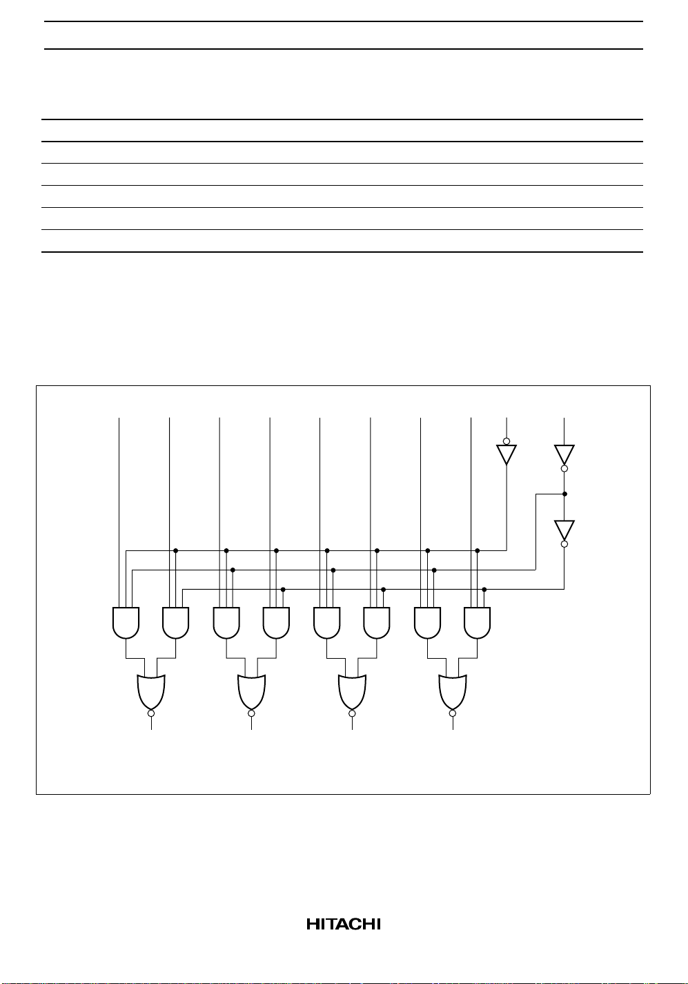
Logic Diagram
I0a I1a I0b I1b I0c I1c I0d I1d SE
Z
Za Zb Zc Zd
Please note that this diagram is provided only for the understanding of logic operations and should not be
used to estimate propagation delays.
3
 Loading...