HIT HD66130T Datasheet

HD66130T
320-channel Low-voltage Segment Driver for Dot-Matrix STN
Liquid Crystal Display
Description
The HD66130T is a 320-channel segment driver for driving a dot-matrix STN liquid-crystal panel at a low
voltage. The driver can also correspond to 240-channel output by switching mode. It operates at a low
voltage: a liquid-crystal drive voltage of 5 V and a logic drive voltage of 3 V, and is used together with
common driver HD66131T or HD66135T. The package, which adopts a flexible TCP, can be applied to
various liquid crystal panels.
Features
• Display duty: Up to 1/240
• Liquid crystal drive voltage: 2.6 to 5.5 V
• Number of liquid crystal drive circuits: 320 circuits
• Operating voltage: 2.5 to 5.5 V
• Number of data bits: 4 or 8 bits
• Shift clock speed: 8 MHz max/5V
6.5 MHz max/3V
• Together with the common drivers
HD66131T , HD66135T
• Low power consumption
• Switching output mode: 320 output mode
240 output mode
• Display-off function
• Flexible TCP
• Automatic generation of chip-enable signals
• Standby function
1

HD66130T
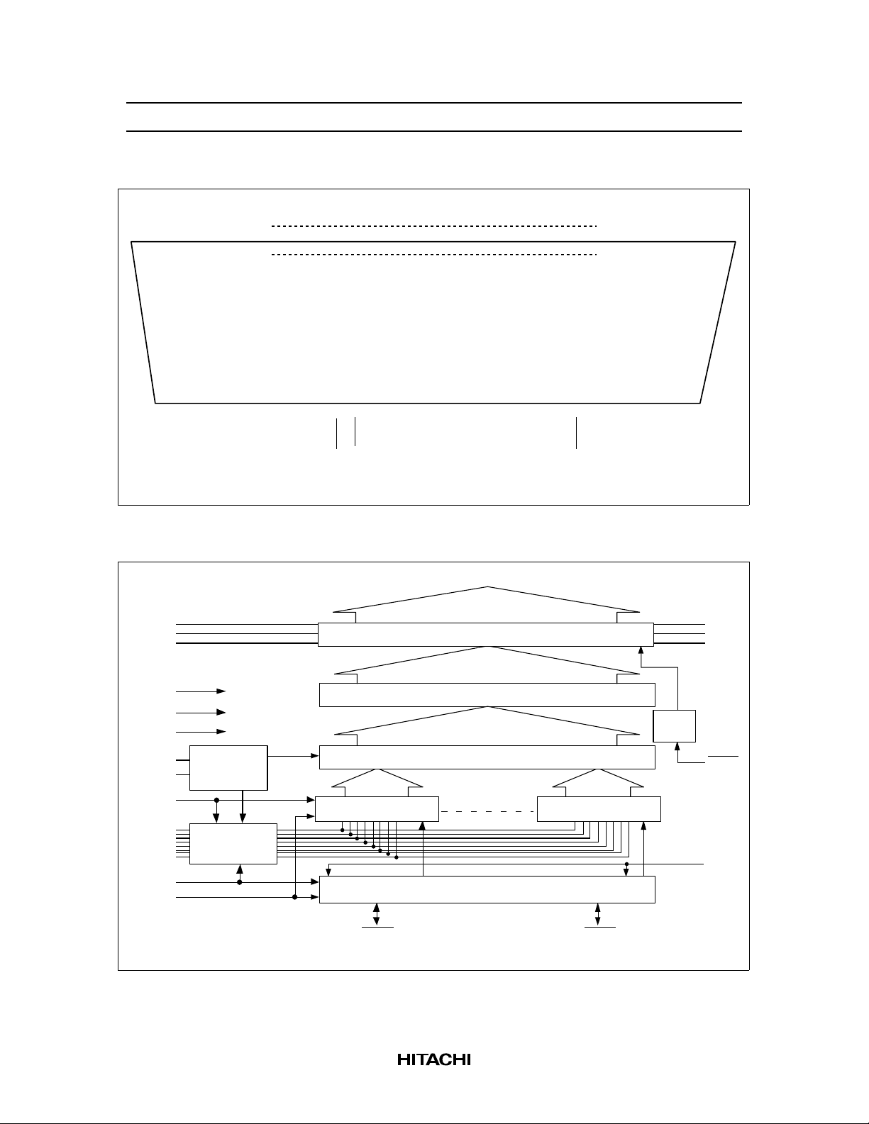
Pin Arrangement
2Y2
3Y3
1 Y1
Note: TCP dimensions are not defined.
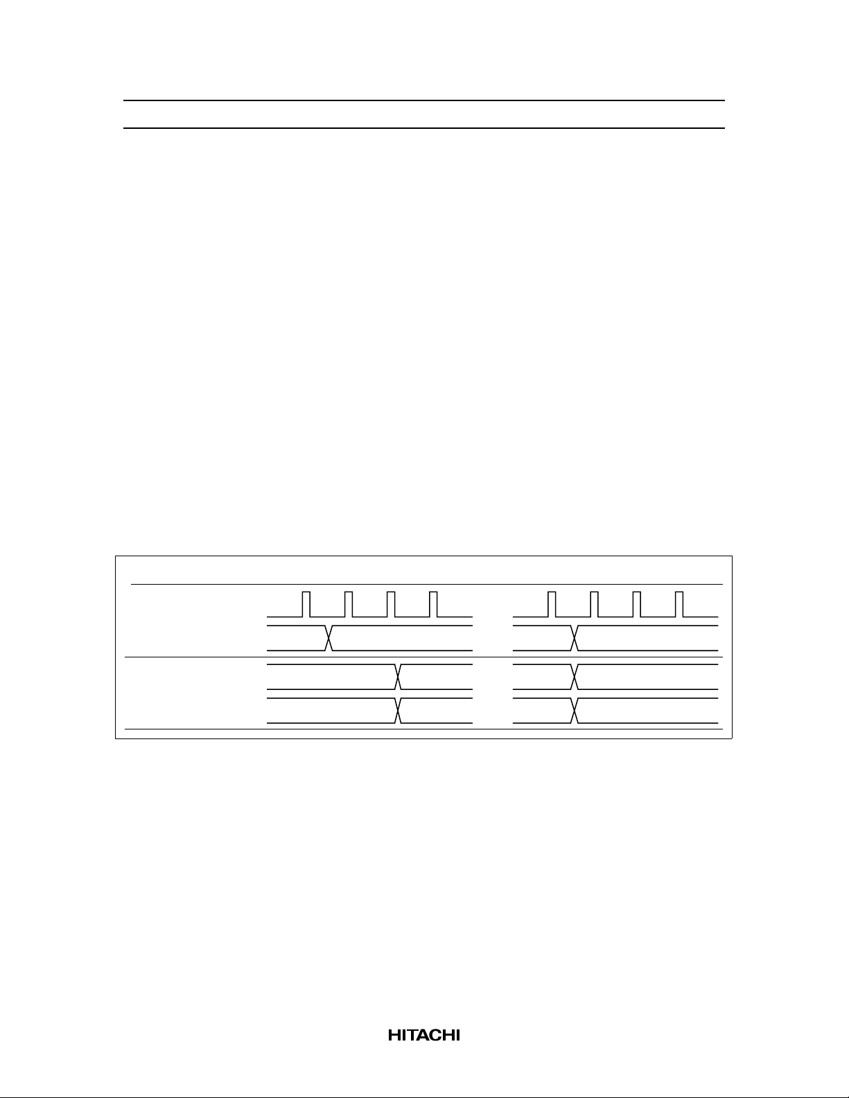
Internal Block Diagram
346
VML
4Y4
5Y5
345
344
343
V0L
V1L
VCCMODEBSGND2
342
341
340
339
SHL
Top View
338
337
336
335
334
333
332
331
EIO1
DISPD0D1D2D3D4D5D6D7
330
329
328
CL2
327
326
325
324
CL1MEIO2
GND1
316 Y316
317 Y317
323
V1R
318 Y318
322
V0R
319 Y319
321
VMR
320 Y320
Y1–Y
320
V0L
VML
V1L
Vcc
GND2
GND1
CL1
M
BS
D0–D7
SHL
MODE
Note: Pins V0L, VML, and V1L are internally connected to pins V0R, VMR, and V1R, respectively.
Timing
generator
circuit
Data
rearrangement
circuit
Liquid crystal drive circuit
Level shifter
Level
shifter
Latch circuit 2
Latch circuit 1Latch circuit 1
Shift register
EIO1 EIO2
*
V0L
VML
V1L
DISP
CL2
2

HD66130T
1. Liquid crystal drive circuit
Selects and outputs the liquid crystal drive level V0, VM, or V1 by DISP and a combination of data for
latch circuit 2 and signal M.
2. Level shifter
Converts logic signals to liquid crystal drive signals.
3. Latch circuit 2
320-bit latch circuit, which latches the data of latch circuits 1 at the fall of CL1 and outputs the data to
the level shifter.
4. Latch circuit 1
4/8-bit parallel data latch circuit, which latches display data D0 to D7 according to signals transmitted
from the shift register.
5. Shift register
80-bit shift register, which generates data-capture signals for latch circuits 1 at the fall of CL2.
6. Data rearrangement circuit
Inverts the order of data output crosswise.
7. Timing generator circuit
The timing generator circuit generates data latch pulses for latch circuit2 and changes pulse the LCD
drive outputs to AC.
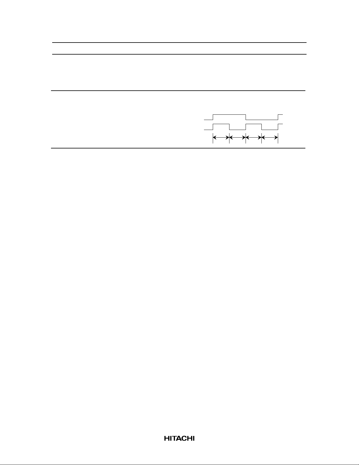
HIFAS Family timing Comparision
HD66130/131/134/135 HD66132/133
Input
CL1
signal
M
Output
signal
Segment
Common
3

HD66130T
Pin Functions
Class Symbol
Power
supply
V
CC
GND1
GND2
V0L, R
VML, R
V1L, R
Control
CL1 327 Clock 1 Input Latch signal of display data: A liquid crystal drive signal
signal
CL2 328 Clock 2 Input Capture signal of display data: Display data is captured
M 326 M Input A.C. signal of liquid crystal drive output
D0 to D7 336 to
SHL 339 Shift Left Input Control signal for inverting the order of data output
EIO1 338 Enable
Pin
Number
343
324
340
345, 322
346, 321
344, 323
329
Pin
Name I/O Functions
V
CC
—V
–GND: Power supply for logic.
CC
GND
V0L, R
Input Liquid crystal drive level power supply
VML, R
V1L, R
corresponding to display data is output at the fall of CL1.
at the fall of CL2.
DATA 0
to
Input
Display data Liquid crystal drive output Liquid crystal display
1 (Vcc level) Selected level ON
DATA 7
(see the following page)
I/O
IO1
SHL
GND
Vcc
V0
VM
V1
OFFNot-selected level0 (GND level)
EI/O1 EI/O2
Enable input
Enable output Enable input
Enable output
EIO2 325 Enable
IO2
I/O Enable input: The enable input of the first IC is
connected to the GND and another is connected to the
enable output of the second IC.
Enable output: Connected to the enable input of the
second IC at cascade output.
DISP 337 Disp off Input Grounding DISP sets liquid crystal drive output Y1–Y320
to the VM level.
BS 341 Bus
Select
Input Switches the number of input bits for the display data.
Vcc
8-bit input mode
GND
4-bit input mode (Captures data from D0–D3. At this
time, connect D4–D7 to the GND.)
MODE 342 MODE Input Switches the number of input bits for the display data.
Vcc
320 output mode
GND
240 output mode (Y41–Y280 are valid output. The
other 80 pins output the not-selected-level signals
synchronized every time; release these pins.)
4

Pin Functions (cont)
HD66130T
Class Symbol
Liquid crystal
drive output
Y1 to
Y320
Pin
Number
1 to 320 Y1 to
Pin
Name I/O Function
Y320
Output Liquid crystal drive output: Selects and outputs level
V0 or V1 according to the combination of the M signal
and display data when DISP is connected to Vcc.
M
D
Output level
1
00
11
V0 V1 V1 V0
0
5
 Loading...