


H8/532 Hardware Manual

Preface
The H8/532 is a high-performance single-chip Hitachi-original microcomputer, featuring a highspeed CPU with 16-bit internal data paths and a full complement of on-chip supporting modules.
The H8/532 is an ideal microcontroller for a wide variety of medium-scale devices, including both
office and industrial equipment and consumer products.
Its highly orthogonal instruction set is designed for fast execution of programs coded in the highlevel C language.
On-chip facilities include large RAM and ROM memories, numerous timers, serial I/O, an A/D
converter, I/O ports, and other functions for compact implementation of high-performance
application systems.
The H8/532 is available in both a ZTAT version* with on-chip PROM, ideal for the early stages
of production or for products with frequently-changing specifications, and a masked-ROM version
suitable for volume production.
This manual gives a hardware description of the H8/532. For details of the instruction set, refer to
the H8/500 Series Programming Manual, which applies to all chips in the H8/500 Series.
* ZTAT (Zero Turn-Around Time) is a registered trademark of Hitachi, Ltd.

Contents
Section 1 Overview
1.1 Features ··································································································································1
1.2 Block Diagram ·······················································································································4
1.3 Pin Arrangements and Functions ···························································································5
1.3.1 Pin Arrangement ·········································································································5
1.3.2 Pin Functions ··············································································································8
Section 2 MCU Operating Modes and Address Space
2.1 Overview ······························································································································23
2.2 Mode Descriptions ···············································································································24
2.3 Address Space Map ··············································································································25
2.3.1 Page Segmentation ····································································································25
2.3.2 Page 0 Address Allocations ······················································································27
2.4 Mode Control Register (MDCR) ·························································································29
Section 3 CPU
3.1 Overview ······························································································································31
3.1.1 Features ·····················································································································31
3.1.2 Address Space ···········································································································32
3.1.3 Register Configuration ······························································································33
3.2 CPU Register Descriptions ··································································································34
3.2.1 General Registers ······································································································34
3.2.2 Control Registers ······································································································35
3.2.3 Initial Register Values ·······························································································40
3.3 Data Formats ························································································································41
3.3.1 Data Formats in General Registers ···········································································41
3.3.2 Data Formats in Memory ··························································································42
3.4 Instructions ···························································································································44
3.4.1 Basic Instruction Formats ·························································································44
3.4.2 Addressing Modes ····································································································45
3.4.3 Effective Address Calculation ···················································································47
3.5 Instruction Set ······················································································································50
3.5.1 Overview ···················································································································50
3.5.2 Data Transfer Instructions ·························································································52
3.5.3 Arithmetic Instructions ·····························································································53
3.5.4 Logic Operations ·······································································································54
3.5.5 Shift Operations ········································································································55
3.5.6 Bit Manipulations ······································································································56
3.5.7 Branching Instructions ······························································································57

3.5.8 System Control Instructions ······················································································59
3.5.9 Short-Format Instructions ·························································································62
3.6 Operating Modes ··················································································································62
3.6.1 Minimum Mode ········································································································62
3.6.2 Maximum Mode ········································································································63
3.7 Basic Operational Timing ····································································································63
3.7.1 Overview ···················································································································63
3.7.2 On-Chip Memory Access Cycle ···············································································64
3.7.3 Pin States during On-Chip Memory Access ·····························································65
3.7.4 Register Field Access Cycle (Addresses H'FF80 to H'FFFF) ···································66
3.7.5 Pin States during Register Field Access (Addresses H'FF80 to H'FFFF) ·················67
3.7.6 External Access Cycle ·······························································································68
3.8 CPU States ···························································································································69
3.8.1 Overview ···················································································································69
3.8.2 Program Execution State ···························································································71
3.8.3 Exception-Handling State ·························································································71
3.8.4 Bus-Released State ····································································································72
3.8.5 Reset State ·················································································································77
3.8.6 Power-Down State ····································································································77
3.9 Programming Notes ·············································································································78
3.9.1 Restriction on Address Location ···············································································78
3.9.2 Note on MULXU Instruction·····················································································79
Section 4 Exception Handling
4.1 Overview ······························································································································81
4.1.1 Types of Exception Handling and Their Priority ······················································81
4.1.2 Hardware Exception-Handling Sequence ·································································82
4.1.3 Exception Factors and Vector Table ··········································································82
4.2 Reset ····································································································································85
4.2.1 Overview ···················································································································85
4.2.2 Reset Sequence ·········································································································85
4.2.3 Stack Pointer Initialization ························································································86
4.3 Address Error ·······················································································································89
4.3.1 Illegal Instruction Prefetch ························································································89
4.3.2 Word Data Access at Odd Address ···········································································89
4.3.3 Off-Chip Address Access in Single-Chip Mode ·······················································89
4.4 Trace ····································································································································90
4.5 Interrupts ······························································································································90
4.6 Invalid Instruction ················································································································92
4.7 Trap Instructions and Zero Divide ·······················································································92
4.8 Cases in Which Exception Handling is Deferred ·································································92

4.8.1 Instructions that Disable Interrupts ···········································································92
4.8.2 Disabling of Exceptions Immediately after a Reset ··················································93
4.8.3 Disabling of Interrupts after a Data Transfer Cycle ··················································93
4.9 Stack Status after Completion of Exception Handling ························································94
4.9.1 PC Value Pushed on Stack for Trace,
Interrupts, Trap Instructions, and Zero Divide Exceptions ·······································96
4.9.2 PC Value Pushed on Stack for Address Error and Invalid
Instruction Exceptions ······························································································96
4.10 Notes on Use of the Stack ····································································································96
Section 5 Interrupt Controller
5.1 Overview ······························································································································97
5.1.1 Features ·····················································································································97
5.1.2 Block Diagram ··········································································································98
5.1.3 Register Configuration ······························································································99
5.2 Interrupt Types ·····················································································································99
5.2.1 External Interrupts ····································································································99
5.2.2 Internal Interrupts ····································································································101
5.2.3 Interrupt Vector Table ·····························································································101
5.3 Register Descriptions ·········································································································103
5.3.1 Interrupt Priority Registers A to D (IPRA to IPRD) ···············································103
5.3.2 Timing of Priority Setting ·······················································································104
5.4 Interrupt Handling Sequence ·····························································································104
5.4.1 Interrupt Handling Flow ··························································································104
5.4.2 Stack Status after Interrupt Handling Sequence ·····················································107
5.4.3 Timing of Interrupt Exception-Handling Sequence ················································108
5.5 Interrupts During Operation of the Data Transfer Controller ············································108
5.6 Interrupt Response Time ····································································································111
Section 6 Data Transfer Controller
6.1 Overview ····························································································································113
6.1.1 Features ···················································································································113
6.1.2 Block Diagram ········································································································113
6.1.3 Register Configuration ····························································································114
6.2 Register Descriptions ·········································································································115
6.2.1 Data Transfer Mode Register (DTMR) ···································································115
6.2.2 Data Transfer Source Address Register (DTSR) ····················································116
6.2.3 Data Transfer Destination Register (DTDR) ·························································116
6.2.4 Data Transfer Count Register (DTCR) ···································································116
6.2.5 Data Transfer Enable Registers A to D (DTEA to DTED) ·····································117
6.3 Data Transfer Operation ·····································································································118

6.3.1 Data Transfer Cycle ································································································118
6.3.2 DTC Vector Table ···································································································120
6.3.3 Location of Register Information in Memory ·························································122
6.3.4 Length of Data Transfer Cycle ················································································122
6.4 Procedure for Using the DTC ····························································································124
6.5 Example ·····························································································································125
Section 7 Wait-State Controller
7.1 Overview ····························································································································127
7.1.1 Features ···················································································································127
7.1.2 Block Diagram ········································································································128
7.1.3 Register Configuration ····························································································128
7.2 Wait-State Control Register ·······························································································129
7.3 Operation in Each Wait Mode ····························································································130
7.3.1 Programmable Wait Mode ······················································································130
7.3.2 Pin Wait Mode ········································································································131
7.3.3 Pin Auto-Wait Mode ·······························································································133
Section 8 Clock Pulse Generator
8.1 Overview ····························································································································135
8.1.1 Block Diagram ········································································································135
8.2 Oscillator Circuit ················································································································135
8.3 System Clock Divider ········································································································138
Section 9 I/O Ports
9.1 Overview ····························································································································139
9.2 Port 1 ··································································································································142
9.2.1 Overview ·················································································································142
9.2.2 Port 1 Registers ·······································································································142
9.2.3 Pin Functions in Each Mode ···················································································145
9.3 Port 2 ··································································································································148
9.3.1 Overview ·················································································································148
9.3.2 Port 2 Registers ·······································································································149
9.3.3 Pin Functions in Each Mode ···················································································150
9.4 Port 3 ··································································································································151
9.4.1 Overview ·················································································································151
9.4.2 Port 3 Registers ·······································································································152
9.4.3 Pin Functions in Each Mode ···················································································153
9.5 Port 4 ··································································································································154
9.5.1 Overview ·················································································································154
9.5.2 Port 4 Registers ·······································································································155

9.5.3 Pin Functions in Each Mode ···················································································156
9.6 Port 5 ··································································································································157
9.6.1 Overview ·················································································································157
9.6.2 Port 5 Registers ·······································································································158
9.6.3 Pin Functions in Each Mode ···················································································159
9.6.4 Built-in MOS Pull-Up ·····························································································161
9.7 Port 6 ··································································································································163
9.7.1 Overview ·················································································································163
9.7.2 Port 6 Registers ·······································································································164
9.7.3 Pin Functions in Each Mode ···················································································165
9.7.4 Built-in MOS Pull-Up ·····························································································167
9.8 Port 7 ··································································································································167
9.8.1 Overview ·················································································································167
9.8.2 Port 7 Registers ·······································································································168
9.8.3 Pin Functions ··········································································································169
9.9 Port 8 ··································································································································172
9.9.1 Overview ·················································································································172
9.9.2 Port 8 Registers ·······································································································172
9.10 Port 9 ··································································································································173
9.10.1 Overview ·················································································································173
9.10.2 Port 9 Registers ·······································································································173
9.10.3 Pin Functions ··········································································································174
Section 10 16-Bit Free-Running Timers
10.1 Overview ····························································································································177
10.1.1 Features ···················································································································177
10.1.2 Block Diagram ········································································································178
10.1.3 Input and Output Pins ·····························································································179
10.1.4 Register Configuration ····························································································180
10.2 Register Descriptions ·········································································································181
10.2.1 Free-Running Counter (FRC) - H'FF92, H'FFA2, H'FFB2 ····································181
10.2.2 Output Compare Registers A and B (OCRA and OCRB) - H'FF94
and H'FF96, H'FFA4 and H'FFA6, H'FFB4 and H'FFB6 ·······································182
10.2.3 Input Capture Register (ICR) - H'FF98, H'FFA8, H'FFB8 ·····································182
10.2.4 Timer Control Register (TCR) ················································································183
10.2.5 Timer Control/Status Register (TCSR) ···································································185
10.3 CPU Interface ·····················································································································188
10.4 Operation ····························································································································190
10.4.1 FRC Incrementation Timing ···················································································190
10.4.2 Output Compare Timing ·························································································191
10.4.3 Input Capture Timing ······························································································193

10.4.4 Setting of FRC Overflow Flag (OVF) ·····································································195
10.5 CPU Interrupts and DTC Interrupts ···················································································195
10.6 Synchronization of Free-Running Timers 1 to 3 ································································196
10.6.1 Synchronization after a Reset ·················································································196
10.6.2 Synchronization by Writing to FRCs ······································································196
10.7 Sample Application ············································································································200
10.8 Application Notes ··············································································································200
Section 11 8-Bit Timer
11.1 Overview ····························································································································207
11.1.1 Features ···················································································································207
11.1.2 Block Diagram ········································································································208
11.1.3 Input and Output Pins ·····························································································209
11.1.4 Register Configuration ····························································································209
11.2 Register Descriptions ·········································································································209
11.2.1 Timer Counter (TCNT) - H'FFD4 ···········································································209
11.2.2 Time Constant Registers A and B
(TCORA and TCORB) - H'FFD2 and H'FFD3 ······················································210
11.2.3 Timer Control Register (TCR) - H'FFD0 ································································210
11.2.4 Timer Control/Status Register (TCSR) ···································································212
11.3 Operation ····························································································································214
11.3.1 TCNT Incrementation Timing ················································································214
11.3.2 Compare Match Timing ··························································································215
11.3.3 External Reset of TCNT ·························································································217
11.3.4 Setting of TCNT Overflow Flag ·············································································218
11.4 CPU Interrupts and DTC Interrupts ···················································································218
11.5 Sample Application ············································································································219
11.6 Application Notes ··············································································································220
Section 12 PWM Timer
12.1 Overview ····························································································································227
12.1.1 Features ···················································································································227
12.1.2 Block Diagram ········································································································227
12.1.3 Input and Output Pins ·····························································································228
12.1.4 Register Configuration ····························································································229
12.2 Register Descriptions ·········································································································229
12.2.1 Timer Counter (TCNT) - H'FFC2, H'FFC4, H'FFCA ············································229
12.2.2 Duty Register (DTR) - H'FFC1, H'FFC5, H'FFC9 ·················································230
12.2.3 Timer Control Register (TCR) - H'FFC0, H'FFC4, H'FFC8 ··································230
12.3 Operation ····························································································································232
12.4 Application Notes ··············································································································234

Section 13 Watchdog Timer
13.1 Overview ····························································································································235
13.1.1 Features ···················································································································235
13.1.2 Block Diagram ········································································································236
13.1.3 Register Configuration ····························································································236
13.2 Register Descriptions ·········································································································237
13.2.1 Timer Counter TCNT - H'FFED ·············································································237
13.2.2 Timer Control/Status Register (TCSR) - H'FFEC (Read), H'FFED (Write) ··········237
13.2.3 Notes on Register Access ························································································239
13.3 Operation ····························································································································240
13.3.1 Watchdog Timer Mode ···························································································240
13.3.2 Interval Timer Mode ·······························································································241
13.3.3 Operation in Software Standby Mode ·····································································242
13.3.4 Setting of Overflow Flag ·························································································243
13.4 Application Notes ··············································································································243
Section 14 Serial Communication Interface
14.1 Overview ····························································································································245
14.1.1 Features ···················································································································245
14.1.2 Block Diagram ········································································································246
14.1.3 Input and Output Pins ·····························································································247
14.1.4 Register Configuration ····························································································247
14.2 Register Descriptions ·········································································································247
14.2.1 Receive Shift Register (RSR) ··················································································247
14.2.2 Receive Data Register (RDR) - H'FFDD ································································248
14.2.3 Transmit Shift Register (TSR) ················································································248
14.2.4 Transmit Data Register (TDR) - H'FFDB ·······························································248
14.2.5 Serial Mode Register (SMR) - H'FFD8 ··································································249
14.2.6 Serial Control Register (SCR) - H'FFDA ·······························································251
14.2.7 Serial Status Register (SSR) - H'FFDC ··································································253
14.2.8 Bit Rate Register (BRR) - H'FFD9 ·········································································255
14.3 Operation ····························································································································259
14.3.1 Overview ·················································································································259
14.3.2 Asynchronous Mode ·······························································································260
14.3.3 Synchronous Mode ·································································································264
14.4 CPU Interrupts and DTC Interrupts ···················································································268
14.5 Application Notes ··············································································································269
Section 15 A/D Converter
15.1 Overview ····························································································································273

15.1.1 Features ···················································································································273
15.1.2 Block Diagram ········································································································274
15.1.3 Input Pins ················································································································275
15.1.4 Register Configuration ····························································································275
15.2 Register Descriptions ·········································································································276
15.2.1 A/D Data Registers (ADDR) - H'FFE0 to H'FFE7 ·················································276
15.2.2 A/D Control/Status Register (ADCSR) - H'FFE8 ··················································277
15.3 CPU Interface ·····················································································································279
15.4 Operation ····························································································································280
15.4.1 Single Mode ············································································································281
15.4.2 Scan Mode ··············································································································284
15.5 Input Sampling Time and A/D Conversion Time ·······························································287
15.6 Interrupts and the Data Transfer Controller ·······································································289
Section 16 RAM
16.1 Overview ····························································································································291
16.1.1 Block Diagram ········································································································291
16.1.2 Register Configuration ····························································································292
16.2 RAM Control Register (RAMCR) ·····················································································292
16.3 Operation ····························································································································292
16.3.1 Expanded Modes (Modes 1, 2, 3, and 4) ································································292
16.3.2 Single-Chip Mode (Mode 7) ···················································································293
Section 17 ROM
17.1 Overview ····························································································································295
17.1.1 Block Diagram ········································································································295
17.2 PROM Modes ·····················································································································296
17.2.1 PROM Mode Setup ·································································································296
17.2.2 Socket Adapter Pin Arrangements and Memory Map ············································297
17.3 Programming ······················································································································299
17.3.1 Writing and Verifying ·····························································································299
17.3.2 Notes on Writing ·····································································································302
17.3.3 Reliability of Written Data ······················································································303
17.3.4 Erasing of Data ·······································································································304
17.4 Handling of Windowed Packages ······················································································304
Section 18 Power-Down State
18.1 Overview ····························································································································307
18.2 Sleep Mode ························································································································308
18.2.1 Transition to Sleep Mode ························································································308
18.2.2 Exit from Sleep Mode ·····························································································308

18.3 Software Standby Mode ·····································································································308
18.3.1 Transition to Software Standby Mode ····································································308
18.3.2 Software Standby Control Register (SBYCR) ························································309
18.3.3 Exit from Software Standby Mode ·········································································310
18.3.4 Sample Application of Software Standby Mode ····················································310
18.3.5 Application Notes ···································································································311
18.4 Hardware Standby Mode ····································································································312
18.4.1 Transition to Hardware Standby Mode ···································································312
18.4.2 Recovery from Hardware Standby Mode ·······························································312
18.4.3 Timing Sequence of Hardware Standby Mode ·······················································313
Section 19 E Clock Interface
19.1 Overview ····························································································································315
Section 20 Electrical Specifications
20.1 Absolute Maximum Ratings ······························································································319
20.2 Electrical Characteristics ····································································································319
20.2.1 DC Characteristics ··································································································319
20.2.2 AC Characteristics ··································································································322
20.2.3 A/D Converter Characteristics ················································································326
20.3 MCU Operatinal Timing ····································································································326
20.3.1 Bus Timing ··············································································································327
20.3.2 Control Signal Timing ····························································································330
20.3.3 Clock Timing ··········································································································331
20.3.4 I/O Port Timing ·······································································································333
20.3.5 16-Bit Free-Running Timer Timing ········································································334
20.3.6 8-Bit Timer Timing ·································································································335
20.3.7 Pulse Width Modulation Timer Timing ··································································336
20.3.8 Serial Communication Interface Timing ·································································336
Appendix A Instructions
A.1 Instruction Set ····················································································································337
A.2 Instruction Codes ···············································································································342
A.3 Operation Code Map ··········································································································353
A.4 Instruction Execution Cycles ·····························································································358
A.4.1 Calculation of Instruction Execution States ····························································358
A.4.2 Tables of Instruction Execution Cycles ··································································359
Appendix B Register Field
B.1 Register Addresses and Bit Names ····················································································367
B.2 Register Descriptions ·········································································································372

Appendix C I/O Port Schematic Diagrams
C.1 Schematic Diagram of Port 1 ·····························································································407
C.2 Schematic Diagram of Port 2 ·····························································································413
C.3 Schematic Diagram of Port 3 ·····························································································414
C.4 Schematic Diagram of Port 4 ·····························································································415
C.5 Schematic Diagram of Port 5 ·····························································································416
C.6 Schematic Diagram of Port 6 ·····························································································417
C.7 Schematic Diagram of Port 7 ·····························································································418
C.8 Schematic Diagram of Port 8 ·····························································································423
C.9 Schematic Diagram of Port 9 ·····························································································424
Appendix D Memory Map ·································································································429
Appendix E Pin State
E.1 Port State of Each Pin State ·······························································································431
E.2 Pin Stattus in the Reset State ······························································································434
Appendix F
Timing of Entry to and Recovery from Hardware Standby Mode
········449
Appendix G Package Dimensions ····················································································451

Figures
1-1 Block Diagram ···················································································································4
1-2 Pin Arrangement (CP-84, Top View) ·················································································5
1-3 Pin Arrangement (CG-84, Top View) ················································································6
1-4 Pin Arrangement (FP-80A, Top View) ··············································································7
2-1 Address Space in Each Mode ··························································································26
2-2 Map of Page 0 ··················································································································28
3-1 CPU Operating Modes ·····································································································32
3-2 Registers in the CPU ········································································································33
3-3 Stack Pointer ····················································································································34
3-4 Combinations of Page Registers with Other Registers ····················································38
3-5 Short Absolute Addressing Mode and Base Register ······················································39
3-6 On-Chip Memory Access Timing ····················································································64
3-7 Pin States during Access to On-Chip Memory ································································65
3-8 Register Field Access Timing ··························································································66
3-9 Pin States during Register Field Access ··········································································67
3-10 (a) External Access Cycle (Read Access) ·············································································68
3-10 (b) External Access Cycle (Write Access) ············································································69
3-11 Operating States ···············································································································70
3-12 State Transitions ··············································································································71
3-13 Bus-Right Release Cycle (During On-chip Memory Access Cycle) ·······························73
3-14 Bus-Right Release Cycle (During External Access Cycle) ·············································74
3-15 Bus-Right Release Cycle (During Internal CPU Operation) ···········································75
4-1 Types of Factors Causing Exception Handling ································································83
4-2 Reset Vector ·····················································································································86
4-3 Reset Sequence (Minimum Mode, On-Chip Memory) ···················································87
4-4 Reset Sequence (Maximum Mode, External Memory) ···················································88
4-5 Interrupt Sources (and Number of Interrupt Types) ························································91
5-1 Interrupt Controller Block Diagram ················································································98
5-2 Interrupt Handling Flowchart ························································································106
5-3 (a) Stack before and after Interrupt Exception-Handling (Minimum Mode) ······················107
5-3 (b) Stack before and after Interrupt Exception-Handling (Maximum Mode) ·····················108
5-4 Interrupt Sequence (Minimum Mode, On-Chip Memory) ············································109
5-5 Interrupt Sequence (Maximum Mode, External Memory) ············································110
6-1 Block Diagram of Data Transfer Controller ··································································114
6-2 Flowchart of Data Transfer Cycle ··················································································119
6-3 DTC Vector Table ··········································································································120
6-4 DTC Vector Table Entry ································································································121
6-5 Order of Register Information ·······················································································122
6-6 Use of DTC to Receive Data via Serial Communication Interface ·······························126
7-1 Block Diagram of Wait-State Controller ·······································································128

7-2 Programmable Wait Mode ·····························································································131
7-3 Pin Wait Mode ···············································································································132
7-4 Pin Auto-Wait Mode ······································································································133
8-1 Block Diagram of Clock Pulse Generator ·····································································135
8-2 Connection of Crystal Oscillator (Example) ·································································136
8-3 Crystal Oscillator Equivalent Circuit ·············································································136
8-4 Notes on Board Design around External Crystal ···························································137
8-5 External Clock Input (Example) ····················································································137
8-6 Phase Relationship of ø Clock and E clock ···································································138
9-1 Pin Functions of Port 1 ··································································································142
9-2 Pin Functions of Port 2 ··································································································148
9-3 Port 2 Pin Functions in Expanded Modes ······································································150
9-4 Port 2 Pin Functions in Single-Chip Mode ····································································151
9-5 Pin Functions of Port 3 ··································································································151
9-6 Port 3 Pin Functions in Expanded Modes ······································································153
9-7 Port 3 Pin Functions in Single-Chip Mode ····································································154
9-8 Pin Functions of Port 4 ··································································································154
9-9 Port 4 Pin Functions in Expanded Modes ······································································156
9-10 Port 4 Pin Functions in Single-Chip Mode ····································································157
9-11 Pin Functions of Port 5 ··································································································157
9-12 Port 5 Pin Functions in Modes 1 and 3 ··········································································159
9-13 Port 5 Pin Functions in Modes 2 and 4 ··········································································160
9-14 Port 5 Pin Functions in Single-Chip Mode ····································································160
9-15 Pin Functions of Port 6 ··································································································164
9-16 Port 6 Pin Functions in Mode 3 ·····················································································166
9-17 Port 6 Pin Functions in Mode 4 ·····················································································166
9-18 Port 6 Pin Functions in Modes 7, 2, and 1 ·····································································167
9-19 Pin Functions of Port 7 ··································································································168
9-20 Pin Functions of Port 8 ··································································································172
9-21 Pin Functions of Port 9 ··································································································173
10-1 Block Diagram of 16-Bit Free-Running Timer ·····························································178
10-2 (a) Write Access to FRC (When CPU Writes H'AA55) ·····················································189
10-2 (b) Read Access to FRC (When FRC Contains H'AA55) ···················································190
10-3 Increment Timing for External Clock Input ··································································191
10-4 Setting of Output Compare Flags ··················································································192
10-5 Timing of Output Compare A ························································································192
10-6 Clearing of FRC by Compare-Match A ·········································································193
10-7 Input Capture Timing (Usual Case) ···············································································193
10-8 Input Capture Timing (1-State Delay) ···········································································194
10-9 Setting of Input Capture Flag ························································································194
10-10 Setting of Overflow Flag (OVF) ····················································································195

10-11 Square-Wave Output (Example) ····················································································200
10-12 FRC Write-Clear Contention ·························································································201
10-13 FRC Write-Increment Contention ·················································································202
10-14 Contention between OCR Write and Compare-Match ··················································203
11-1 Block Diagram of 8-Bit Timer ·······················································································208
11-2 Count Timing for External Clock Input ·········································································215
11-3 Setting of Compare-Match Flags ···················································································216
11-4 Timing of Timer Output ·································································································216
11-5 Timing of Compare-Match Clear ··················································································217
11-6 Timing of External Reset ·······························································································217
11-7 Setting of Overflow Flag (OVF) ····················································································218
11-8 Example of Pulse Output ·······························································································219
11-9 TCNT Write-Clear Contention ······················································································220
11-10 TCNT Write-Increment Contention ··············································································221
11-11 Contention between TCOR Write and Compare-Match ···············································222
12-1 Block Diagram of PWM Timer ·····················································································228
12-2 PWM Timing ·················································································································233
13-1 Block Diagram of Timer Counter ··················································································236
13-2 Writing to TCNT and TCSR ··························································································239
13-3 Operation in Watchdog Timer Mode ·············································································241
13-4 Operation in Interval Timer Mode ·················································································242
13-5 Setting of OVF Bit ·········································································································243
13-6 TCNT Write-Increment Contention ··············································································244
14-1 Block Diagram of Serial Communication Interface ······················································246
14-2 Data Format in Asynchronous Mode ·············································································260
14-3 Phase Relationship between Clock Output and Transmit Data ·····································261
14-4 Data Format in Synchronous Mode ···············································································265
14-5 Sampling Timing (Asynchronous Mode) ······································································271
15-1 Block Diagram of A/D Converter ··················································································274
15-2 Read Access to A/D Data Register (When Register Contains H'AA40) ·······················280
15-3 A/D Operation in Single Mode (When Channel 1 is Selected) ·····································283
15-4 A/D Operation in Scan Mode (When Channels 0 to 2 are Selected) ·····························286
15-5 A/D Conversion Timing ·································································································288
16-1 Block Diagram of On-Chip RAM ·················································································291
17-1 Block Diagram of On-Chip ROM ·················································································296
17-2 Socket Adapter Pin Arrangements ·················································································298
17-3 Memory Map in PROM Mode ·······················································································299
17-4 High-Speed Programming Flowchart ············································································300
17-5 PROM Write/Verify Timing ··························································································302
17-6 Recommended Screening Procedure ·············································································303
18-1 NMI Timing of Software Standby Mode (Application Example) ·································311

18-2 Hardware Standby Sequence ·························································································313
19-1 Execution Cycle of Instruction Synchronized with E Clock in Expanded Modes
(Maximum Synchronization Delay) ··············································································316
19-2 Execution Cycle of Instruction Synchronized with E Clock in Expanded Modes
(Minimum Synchronization Delay) ···············································································317
20-1 Example of Circuit for Driving a Darlington Transistor Pair ········································322
20-2 Example of Circuit for Driving an LED ········································································322
20-3 Output Load Circuit ·······································································································325
20-4 Basic Bus Cycle (without Wait States) in Expanded Modes ·········································327
20-5 Basic Bus Cycle (with 1 Wait State) in Expanded Modes ·············································328
20-6 Bus Cycle Synchronized with E Clock ··········································································329
20-7 Reset Input Timing········································································································ 330
20-8 Interrupt Input Timing ···································································································330
20-9 NMI Pulse Width (for Recovery from Software Standby Mode) ··································330
20-10 Bus Release State Timing ······························································································331
20-11 E Clock Timing ··············································································································331
20-12 Clock Oscillator Stabilization Timing ···········································································332
20-13 I/O Port Input/Output Timing ························································································333
20-14 Free-Running Timer Input/Output Timing ····································································334
20-15 External Clock Input Timing for Free-Running Timers ················································334
20-16 8-Bit Timer Output Timing ····························································································335
20-17 8-Bit Timer Clock Input Timing ····················································································335
20-18 8-Bit Timer Reset Input Timing ····················································································335
20-19 PWM Timer Output Timing ··························································································336
20-20 SCI Input Clock Timing ································································································336
20-21 SCI Input/Output Timing (Synchronous Mode) ····························································336
C-1 (a) Schematic Diagram of Port 1, Pin P10 ··········································································407
C-1 (b) Schematic Diagram of Port 1, Pin P11 ··········································································407
C-1 (c) Schematic Diagram of Port 1, Pin P12 ···········································································408
C-1 (d) Schematic Diagram of Port 1, Pin P13 ··········································································409
C-1 (e) Schematic Diagram of Port 1, Pin P14 ···········································································410
C-1 (f) Schematic Diagram of Port 1, Pins P15 and P16 ···························································411
C-1 (g) Schematic Diagram of Port 1, Pin P17 ··········································································412
C-2 Schematic Diagram of Port 2 ·························································································413
C-3 Schematic Diagram of Port 3 ·························································································414
C-4 Schematic Diagram of Port 4 ·························································································415
C-5 Schematic Diagram of Port 5 ·························································································416
C-6 Schematic Diagram of Port 6 ·························································································417
C-7 (a) Schematic Diagram of Port 7, Pin P70 ··········································································418
C-7 (b) Schematic Diagram of Port 7, Pins P71 and P72 ···························································419
C-7 (c) Schematic Diagram of Port 7, Pin P73 ··········································································420

C-7 (d) Schematic Diagram of Port 7, Pins P74, P75 and P76 ····················································421
C-7 (e) Schematic Diagram of Port 7, Pin P77 ··········································································422
C-8 Schematic Diagram of Port 8 ·························································································423
C-9 (a) Schematic Diagram of Port 9, Pins P90 and P91 ···························································424
C-9 (b) Schematic Diagram of Port 9, Pins P92, P93 and P94 ····················································425
C-9 (c) Schematic Diagram of Port 9, Pin P95 ··········································································426
C-9 (d) Schematic Diagram of Port 9, Pin P96 ··········································································427
C-9 (e) Schematic Diagram of Port 9, Pin P97 ··········································································428
E-1 Reset during Memory Access (Mode 1) ········································································435
E-2 Reset during Memory Access (Mode 1) ········································································436
E-3 Reset during Memory Access (Mode 2) ········································································438
E-4 Reset during Memory Access (Mode 2) ········································································439
E-5 Reset during Memory Access (Mode 3) ········································································441
E-6 Reset during Memory Access (Mode 3) ········································································442
E-7 Reset during Memory Access (Mode 4) ········································································444
E-8 Reset during Memory Access (Mode 4) ········································································445
E-9 Reset during Memory Access (Mode 7) ········································································446
E-10 Reset during Memory Access (Mode 7) ········································································447
G-1 Package Dimensions (CP-84) ························································································451
G-2 Package Dimensions (CG-84) ·······················································································451
G-3 Package Dimensions (FP-80A) ······················································································452
Tables
1-1 Features ······························································································································2
1-2 Pin Arrangements in Each Operating Mode (CP-84, CG-84) ···········································8
1-3 Pin Arrangements in Each Operating Mode (FP-80A) ····················································12
1-4 Pin Functions ···················································································································16
2-1 Operating Modes ·············································································································23
2-2 Mode Control Register ····································································································29
3-1 Interrupt Mask Levels ······································································································36
3-2 Interrupt Mask Bits after an Interrupt is Accepted ··························································36
3-3 Initial Values of Registers ································································································41
3-4 General Register Data Formats ························································································42
3-5 Data Formats in Memory ·································································································43
3-6 Data Formats on the Stack ·······························································································44
3-7 Addressing Modes ···········································································································46
3-8 Effective Address Calculation ·························································································47
3-9 Instruction Classification ·································································································50
3-10 Data Transfer Instructions ·······························································································52
3-11 Arithmetic Instructions ····································································································53
3-12 Logic Operation Instructions ···························································································54

3-13 Shift Instructions ··············································································································55
3-14 Bit-Manipulation Instructions ··························································································56
3-15 Branching Instructions ·····································································································57
3-16 System Control Instructions ····························································································59
3-17 Short-Format Instructions and Equivalent General Formats ···········································62
4-1 (a) Exceptions and Their Priority ··························································································81
4-1 (b) Instruction Exceptions ······································································································81
4-2 Exception Vector Table ····································································································84
4-3 Stack after Exception Handling Sequence ·······································································94
5-1 Interrupt Controller Registers ··························································································99
5-2 Interrupts, Vectors, and Priorities ··················································································102
5-3 Assignment of Interrupt Priority Registers ····································································103
5-4 Number of States before Interrupt Service ····································································111
6-1 Internal Control Registers of the DTC ···········································································114
6-2 Data Transfer Enable Registers ·····················································································115
6-3 Assignment of Data Transfer Enable Registers ·····························································117
6-4 Addresses of DTC Vectors ·····························································································121
6-5 Number of States per Data Transfer ··············································································123
6-6 Number of States before Interrupt Service ····································································124
6-7 DTC Control Register Information Set in RAM ···························································125
7-1 Register Configuration ···································································································128
7-2 Wait Modes ····················································································································130
8-1 External Crystal Parameters ··························································································136
9-1 Input/Output Port Summary ··························································································140
9-2 Port 1 Registers ··············································································································142
9-3 Port 1 Pin Functions in Expanded Modes ······································································145
9-4 Port 1 Pin Functions in Single-Chip Modes ··································································147
9-5 Port 2 Registers ··············································································································149
9-6 Port 3 Registers ··············································································································152
9-7 Port 4 Registers ··············································································································155
9-8 Port 5 Registers ··············································································································158
9-9 Status of MOS Pull-Ups for Port 5 ················································································161
9-10 Port 6 Registers ··············································································································164
9-11 Status of MOS Pull-Ups for Port 5 ················································································167
9-12 Port 7 Registers ··············································································································168
9-13 Port 7 Pin Functions ·······································································································170
9-14 Port 8 Registers ··············································································································172
9-15 Port 9 Registers ··············································································································173
9-16 Port 9 Pin Functions ·······································································································175
10-1 Input and Output Pins of Free-Running Timer Module ················································179
10-2 Register Configuration ···································································································180

10-3 Free-Running Timer Interrupts ······················································································195
10-4 Synchronization by Writing to FRCs ············································································196
10-5 Effect of Changing Internal Clock Sources ···································································204
11-1 Input and Output Pins of 8-Bit Timer ············································································209
11-2 8-Bit Timer Registers ·····································································································209
11-3 8-Bit Timer Interrupts ····································································································218
11-4 Priority Order of Timer Output ······················································································223
11-5 Effect of Changing Internal Clock Sources ···································································223
12-1 Output Pins of PWM Timer Module ·············································································228
12-2 PWM Timer Registers ···································································································229
12-3 PWM Timer Parameters for 10MHz System Clock ······················································232
13-1 Register Configuration ···································································································236
13-2 Read Addresses of TCNT and TCSR ············································································240
14-1 SCI Input/Output Pins ····································································································247
14-2 SCI Registers ·················································································································247
14-3 Examples of BRR Settings in Asynchronous Mode (1) ················································255
14-3 Examples of BRR Settings in Asynchronous Mode (2) ················································256
14-3 Examples of BRR Settings in Asynchronous Mode (3) ················································256
14-3 Examples of BRR Settings in Asynchronous Mode (4) ················································257
14-4 Examples of BRR Settings in Synchronous Mode ························································258
14-5 Communication Formats Used by SCI ··········································································259
14-6 SCI Clock Source Selection ···························································································259
14-7 Data Formats in Asynchronous Mode ···········································································261
14-8 Receive Errors ················································································································264
14-9 SCI Interrupts ·················································································································269
14-10 SSR Bit States and Data Transfer When Multiple Receive Errors Occur ·····················270
15-1 A/D Input Pins ···············································································································275
15-2 A/D Registers ·················································································································275
15-3 Assignment of Data Registers to Analog Input Channels ·············································276
15-4 A/D Conversion Time (Single Mode) ············································································288
16-1 RAM Control Register ···································································································292
17-1 ROM Usage in Each MCU Mode ··················································································295
17-2 Selection of PROM Mode ······························································································296
17-3 Socket Adapter ···············································································································297
17-4 Selection of Sub-Modes in PROM Mode ······································································299
17-5 DC Characteristics
(When VCC = 6.0V ±0.25V, VPP = 12.5V ±0.3V, VSS = 0V, Ta = 25˚C ±5˚C) ············301
17-6 AC Characteristics
(When VCC = 6.0V ±0.25V, VPP = 12.5V ±0.3V, Ta = 25˚C ±5˚C) ······························301
17-7 Erasing Conditions ·········································································································304
17-8 Socket for 84-Pin LCC Package ····················································································305

18-1 Power-Down State ·········································································································307
18-2 Software Standby Control Register ···············································································309
20-1 Absolute Maximum Ratings ··························································································319
20-2 DC Characteristics ·········································································································320
20-3 Allowable Output Current Sink Values ·········································································321
20-4 Bus Timing ····················································································································322
20-5 Control Signal Timing ···································································································324
20-6 Timing Conditions of On-Chip Supporting Modules ····················································325
20-7 A/D Converter Characteristics ·······················································································326
A-1 (a) Machine Language Coding [General Format] ·······························································346
A-1 (b) Machine Language Coding [Special Format: Short Format] ·········································350
A-1 (c) Machine Language Coding [Special Format: Branch Instructions] ······························351
A-1 (d) Machine Language Coding [Special Format: System Control Instructions] ·················352
A-2 Operation Codes in Byte 1 ·····························································································353
A-3 Operation Codes in Byte 2 (Axxx) ················································································354
A-4 Operation Codes in Byte 2 (05xx, 15xx, 0Dxx, 1Dxx, Bxxx, Cxxx, Dxxx,
Exxx, Fxxx) ···················································································································355
A-5 Operation Codes in Byte 2 (04xx, 0Cxx) ······································································356
A-6 Operation Codes in Bytes 2 and 3 (11xx, 01xx, 06xx, 07xx, xx00xx) ··························357
A-7 Instruction Execution Cycles (1) ···················································································361
A-7 Instruction Execution Cycles (2) ····················································································362
A-7 Instruction Execution Cycles (3) ····················································································363
A-7 Instruction Execution Cycles (4) ····················································································364
A-7 Instruction Execution Cycles (5) ····················································································365
A-7 Instruction Execution Cycles (6) ····················································································366
A-8 (a) Adjusted Value (Branch Instruction) ·············································································366
A-8 (b) Adjusted Value (Other Instructions by Addressing Modes) ··········································366
C-1 (a) Port 1 Port Read (Pin P10) ·····························································································407
C-1 (b) Port 1 Port Read (Pin P11) ·····························································································408
C-1 (c) Port 1 Port Read (Pin P12) ·····························································································408
C-1 (d) Port 1 Port Read (Pin P13) ·····························································································409
C-1 (e) Port 1 Port Read (Pin P14) ·····························································································410
C-1 (f) Port 1 Port Read (Pins P15, P16) ····················································································411
C-1 (g) Port 1 Port Read (Pin P17) ·····························································································412
C-2 Port 2 Port Read ·············································································································413
C-3 Port 3 Port Read ·············································································································414
C-4 Port 4 Port Read ·············································································································415
C-5 Port 5 Port Read ·············································································································416
C-6 Port 6 Port Read ·············································································································417
C-7 (a) Port 7 Port Read (Pin P70) ·····························································································418
C-7 (b) Port 7 Port Read (Pins P71, P72) ····················································································419

C-7 (c) Port 7 Port Read (Pin P73) ·····························································································420
C-7 (d) Port 7 Port Read (Pins P74–P76) ····················································································421
C-7 (e) Port 7 Port Read (Pin P77) ·····························································································422
C-9 (a) Port 9 Port Read (Pins P90, P91) ····················································································424
C-9 (b) Port 9 Port Read (Pins P92–P94) ····················································································425
C-9 (c) Port 9 Port Read (Pin P95) ·····························································································426
C-9 (d) Port 9 Port Read (Pin P96) ·····························································································427
C-9 (e) Port 9 Port Read (Pin P97) ·····························································································428
E-1 Port State ························································································································431
E-2 Pull-up MOS State ·········································································································433

Section 1 Overview
1.1 Features
The H8/532 is an original Hitachi CMOS microcomputer unit (MCU) comprising a highperformance CPU core plus a full range of supporting functions—an entire system integrated onto
a single chip.
The CPU features a highly orthogonal instruction set that permits addressing modes and data sizes
to be specified independently in each instruction. An internal 16-bit architecture and 16-bit access
to on-chip memory enhance the CPU’s data-processing capability and provide the speed needed
for realtime control applications.
The on-chip supporting functions include RAM, ROM, timers, a serial communication interface
(SCI), A/D conversion, and I/O ports. An on-chip data transfer controller (DTC) can transfer data
in either direction between memory and I/O independently of the CPU.
For the on-chip ROM, a choice is offered between masked ROM and programmable ROM
(PROM). The PROM version can be programmed by the user with a general-purpose PROM
writer.
Table 1-1 lists the main features of the H8/532 chip.
1

Table 1-1 Features
Feature Description
CPU General-register machine
• Eight 16-bit general registers
• Five 8-bit and two 16-bit control registers
High speed
• Maximum clock rate: 10MHz (oscillator frequency: 20MHz)
Expanded operating modes supporting external memory
• Minimum mode: up to 64K-byte address space
• Maximum mode: up to 1M-byte address space
Highly orthogonal instruction set
• Addressing modes and data size can be specified independently for
each instruction
1.5 Addressing modes
• Register-register operations
• Register-memory operations
Instruction set optimized for C language
• Special short formats for frequently-used instructions and addressing modes
Memory • 1K-Byte high-speed RAM on-chip
• 32K-Byte programmable or masked ROM on-chip
16-Bit free- Each channel provides:
running • 1 free-running counter (which can count external events)
timer (FRT) • 2 output-compare registers
(3 channels) • 1 input capture register
8-Bit timer • One 8-bit up-counter (which can count external events)
(1 channel) • 2 time constant registers
PWM timer • Generates pulses with any duty ratio from 0 to 100%
(3 channels) • Resolution: 1/250
Watchdog • An overflow generates a nonmaskable interrupt
timer (WDT) • Can also be used as an interval timer
(1 channel)
2

Table 1-1 Features (cont)
Feature Description
Serial com- • Asynchronous or synchronous mode (selectable)
munication • Full duplex: can send and receive simultaneously
interface (SCI) • Built-in baud rate generator
A/D converter • 10-Bit resolution
• 8 channels, controllable in single mode or scan mode (selectable)
• Sample-and-hold function
I/O ports • 57 Input/output pins (six 8-bit ports, one 5-bit port, one 4-bit port)
• 8 Input-only pins (one 8-bit port)
• Memory-mapped I/O
Interrupt • 3 external interrupt pins (NMI, IRQ
controller • 19 internal interrupts
(INTC) • 8 priority levels
Data transfer Performs bidirectional data transfer between memory and I/O independently
controller (DTC) of the CPU
Wait-state Can insert wait states in access to external memory or I/O
controller (WSC)
Operating 5 MCU operating modes
modes • Expanded minimum modes, supporting up to 64k bytes external memory
with or without using on-chip ROM (Modes 1 and 2)
• Expanded maximum modes, supporting up to 1M byte external memory
with or without using on-chip ROM (Modes 3 and 4)
• Single-chip mode (Mode 7)
3 power-down modes
• Sleep mode
• Software standby mode
• Hardware standby mode
Other features • E clock output available
• Clock generator on-chip
0, IRQ1)
Model Name Package Options ROM
HD6475328CG 84-Pin windowed LCC (CG-84) PROM
HD6475328CP 84-Pin PLCC (CP-84)
HD6475328F 80-Pin QFP (FP-80A)
HD6435328CP 84-Pin PLCC (CP-84) Mask
HD6435328F 80-Pin QFP (FP-80A) ROM
3
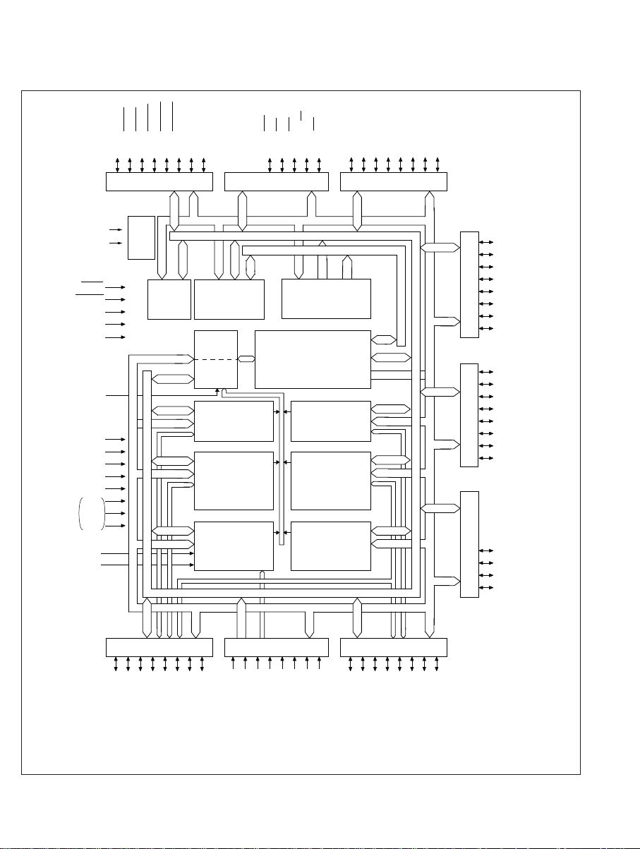
1.2 Block Diagram
CPU
P4 /A
77
P4 /A66
P4 /A55
P4 /A44
P4 /A33
P4 /A22
P4 /A11
P4 /A00
P5 /A157
P5 /A146
P5 /A135
P5 /A124
P5 /A113
P5 /A102
P5 /A91
P5 /A80
P6 /A193
P6 /A182
P6 /A171
P6 /A160
P7 /FTOA17
P7 /FTI22
P7 /FTI11
P7 /TMCI0
P7 /FTOB /FTCI363
P7 /FTOB /FTCI252
P7 /FTOB /FTCI14
P7 /FTI /TMRI33
1
P8 /AN77
P8 /AN66
P8 /AN55
P8 /AN44
P8 /AN33
P8 /AN22
P8 /AN11
P8 /AN00
8 Bits Timer
16 Bits Free
Running Timer
(x 3 channel)
Watchdog
Timer
Serial
Communication
Interface
PWM Timer
(x 3 channel)
10 Bits
A/D Converter
Port 9 Port 8 Port 7
Port 6 Port 5 Port 4
Port 3Port 2Port 1
Clock
Generator
EXTAL
XTAL
WaitState
Controller
RAM
1 kByte
PROM/Mask
ROM 32 kByte
Interrupt
Controller
Data
Transfer
Controller
Vcc
Vcc
Vss
Vss
Vss
Vss
Vss
Vss
*
AV
cc
AVss
NMI
RES
STBY
MD
0
MD1
MD2
P9 /SCK7
P9 /RXD6
P9 /TXD5
P9 /PW34
P9 /PW23
P9 /PW12
P9 /FTOA31
P9 /FTOA20
* CP-84 and CG-84 only
P3 /D77
P3 /D66
P3 /D55
P3 /D44
P3 /D33
P3 /D22
P3 /D11
P3 /D00
P1 /TMO7
P1 /IRQ16
P1 /IRQ05
P1 /WAIT4
P1 /BREQ3
P1 /BACK2
P1 /E1
P1 /ø0
P2 /WR4
P2 /RD3
P2 /DS2
P2 /R/W1
P2 /AS0
Data bus (Low)
Data bus (High)
Address bus
Figure 1-1 shows a block diagram of the H8/532 chip.
Figure 1-1 Block Diagram
4
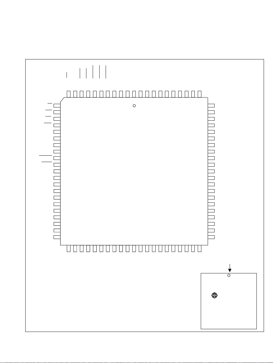
1.3 Pin Arrangements and Functions
1 pin
P2 /R/W
P2 /DS
P2 /RD
P2 /WR
V
MD
MD
MD
STBY
RES
NMI
NC
V
P3 /D
P3 /D
P3 /D
P3 /D
P3 /D
P3 /D
P3 /D
P3 /D
1
2
3
4
cc
0
1
2
ss
0
1
2
3
4
5
6
7
0
1
2
3
4
5
6
7
12
13
14
15
16
17
18
19
20
21
22
23
24
25
26
27
28
29
30
31
32
74
73
72
71
70
69
68
67
66
65
64
63
62
61
60
59
58
57
56
55
54
111098765432184838281807978777675
33 34 35 36 37 38 39 40 41 42 43 44 45 46 47 48 49 50 51 52 53
PLCC-84
H8/532
HD6475328CP
JAPAN
AV
P8 /AN
P8 /AN
P8 /AN
P8 /AN
P8 /AN
P8 /AN
P8 /AN
P8 /AN
AV
V
P7 /FTOA
P7 /FTOB /FTCI
P7 /FTOB /FTCI
P7 /FTOB /FTCI
P7 /FTI /TMRI
P7 /FTI
P7 /FTI
P7 /TMCI
V
P6 /A
cc
77
66
55
44
33
22
11
00
ss
ss
7
6
5
4
3
2
1
0
cc
3
1
3
2
1
3
2
1
3
2
1
19
P2 /AS
P1 /TMO
P1 /IRQ
P1 /IRQ
P1 /WAIT
P1 /BREQ
P1 /BACK
P1 /E
P1 /øVXTAL
EXTALVP9 /SCK
P9 /RXD
P9 /TXD
P9 /PW
P9 /PW
P9 /PW
P9 /FTOA
P9 /FTOA
076543210
ss
ss
7654321
0
321
3
2
1
0
P4 /A
P4 /A
P4 /A
P4 /A
P4 /A
P4 /A
P4 /A
P4 /A
V
V
P5 /A
P5 /A
P5 /A
P5 /A
P5 /A
P5 /A
P5 /A
P5 /A
P6 /A
P6 /A
P6 /A
0123456
7
ss
ss
08
19
210
311
412
513
614
715
013
114
215
0123456
7
1.3.1 Pin Arrangement
Figure 1-2 shows the pin arrangement of the CP-84 package. Figure 1-3 shows the pin
arrangement of the CG-84 package. Figure 1-4 shows the pin arrangement of the FP-80A package.
Figure 1-2 Pin Arrangement (CP-84, Top View)
5
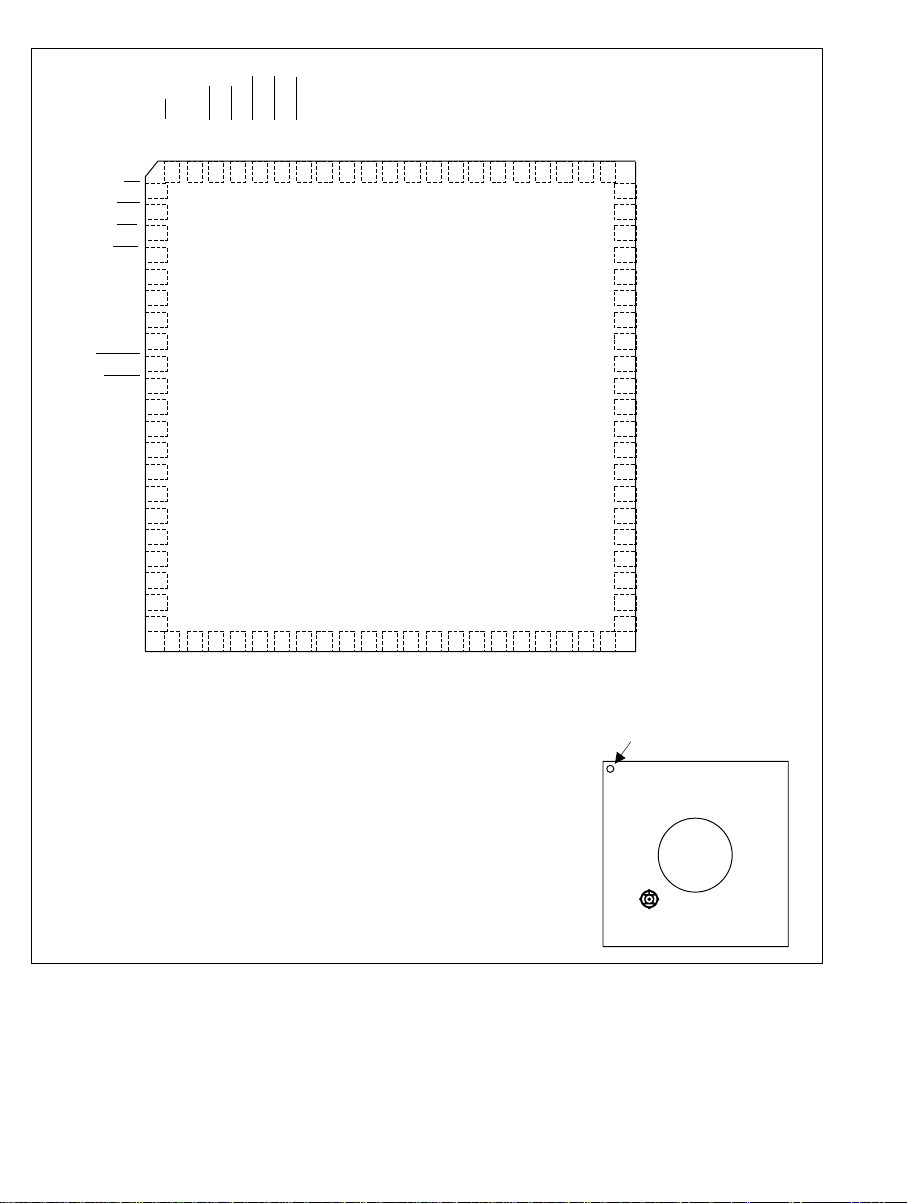
Index
LCC-84
H8/532
HD6475328CG
JAPAN
P2 /R/W
P2 /DS
P2 /RD
P2 /WR
V
MD
MD
MD
STBY
RES
NMI
NC
V
P3 /D
P3 /D
P3 /D
P3 /D
P3 /D
P3 /D
P3 /D
P3 /D
1
2
3
4
cc
0
1
2
ss
0
1
2
3
4
5
6
7
0
1
2
3
4
5
6
7
12
13
14
15
16
17
18
19
20
21
22
23
24
25
26
27
28
29
30
31
32
74
73
72
71
70
69
68
67
66
65
64
63
62
61
60
59
58
57
56
55
54
111098765432184838281807978777675
33 34 35 36 37 38 39 40 41 42 43 44 45 46 47 48 49 50 51 52 53
AV
P8 /AN
P8 /AN
P8 /AN
P8 /AN
P8 /AN
P8 /AN
P8 /AN
P8 /AN
AV
V
P7 /FTOA
P7 /FTOB /FTCI
P7 /FTOB /FTCI
P7 /FTOB /FTCI
P7 /FTI /TMRI
P7 /FTI
P7 /FTI
P7 /TMCI
V
P6 /A
cc
77
66
55
44
33
22
11
00
ss
ss
7
6
5
4
3
2
1
0
cc
3
1
3
2
1
3
2
1
3
2
1
19
P2 /AS
P1 /TMO
P1 /IRQ
P1 /IRQ
P1 /WAIT
P1 /BREQ
P1 /BACK
P1 /E
P1 /øVXTAL
EXTALVP9 /SCK
P9 /RXD
P9 /TXD
P9 /PW
P9 /PW
P9 /PW
P9 /FTOA
P9 /FTOA
076543210
ss
ss
7654321
0
321
3
2
1
0
P4 /A
P4 /A
P4 /A
P4 /A
P4 /A
P4 /A
P4 /A
P4 /A
V
V
P5 /A
P5 /A
P5 /A
P5 /A
P5 /A
P5 /A
P5 /A
P5 /A
P6 /A
P6 /A
P6 /A
0123456
7
ss
ss
08
19
210
311
412
513
614
715
016
117
218
0123456
7
Figure 1-3 Pin Arrangement (CG-84, Top View)
6
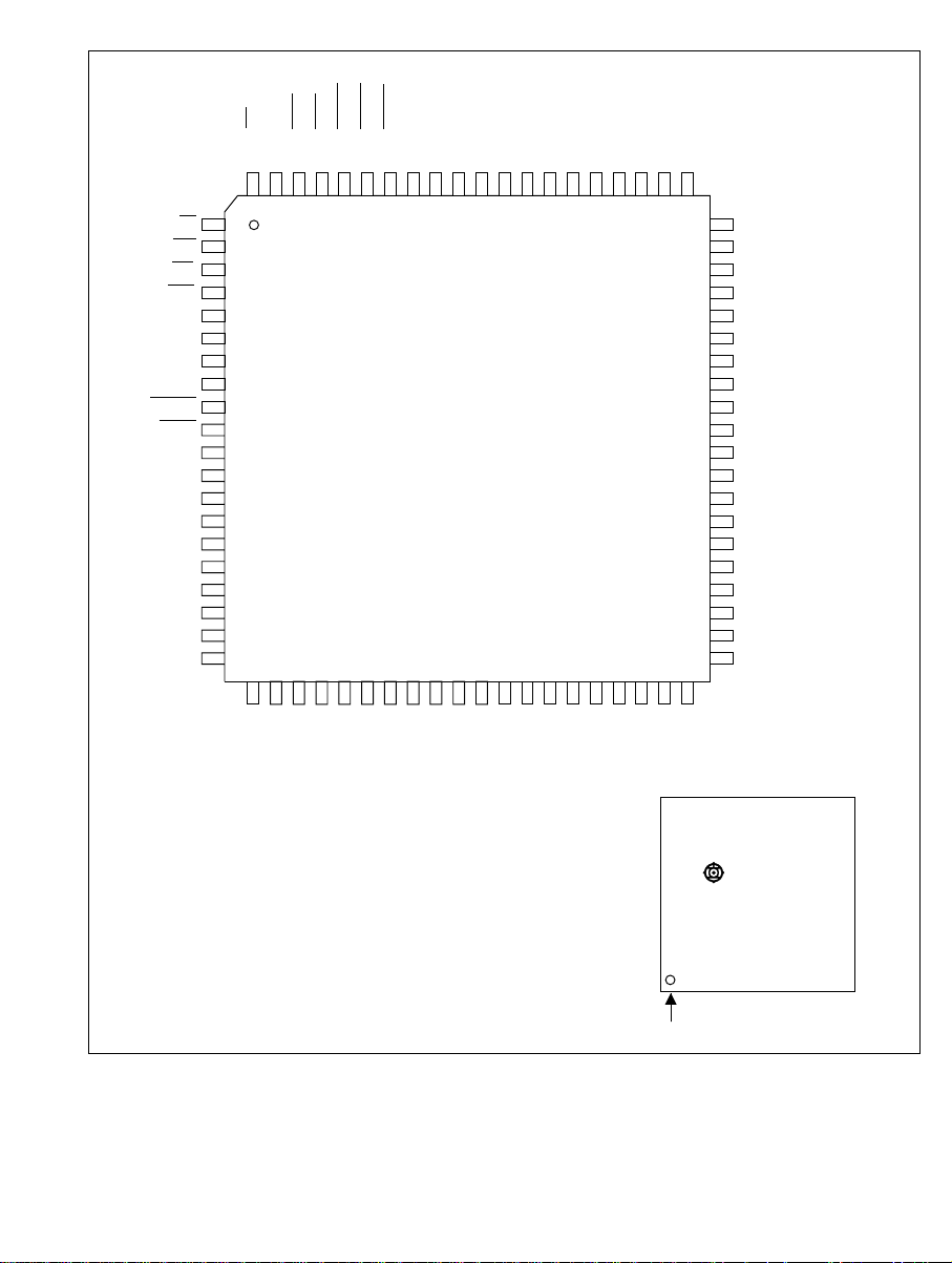
P2 /R/W
P2 /DS
P2 /RD
P2 /WR
V
MD
MD
MD
STBY
RES
NMI
V
P3 /D
P3 /D
P3 /D
P3 /D
P3 /D
P3 /D
P3 /D
P3 /D
1
2
3
4
cc
0
1
2
ss
0
1
2
3
4
5
6
7
0
1
2
3
4
5
6
7
1
2
3
4
5
6
7
8
9
10
11
12
13
14
15
16
17
18
19
20
60
59
58
57
56
55
54
53
52
51
50
49
48
47
46
45
44
43
42
41
80 79 78 77 76 75 74 73 72 71 70 69 68 67 66 65 64 63 62 61
21 22 23 24 25 26 27 28 29 30 31 32 33 34 35 36 37 38 39 40
QFP-80A
H8/532
HD6475328F
JAPAN
AV
P8 /AN
P8 /AN
P8 /AN
P8 /AN
P8 /AN
P8 /AN
P8 /AN
P8 /AN
AV
P7 /FTOA
P7 /FTOB /FTCI
P7 /FTOB /FTCI
P7 /FTOB /FTCI
P7 /FTI /TMRI
P7 /FTI
P7 /FTI
P7 /TMCI
V
P6 /A
cc
77
66
55
44
33
22
11
00
ss
7
6
5
4
3
2
1
0
cc
3
1
3
2
1
3
2
1
3
2
1
19
P2 /AS
P1 /TMO
P1 /IRQ
P1 /IRQ
P1 /WAIT
P1 /BREQ
P1 /BACK
P1 /E
P1 /øVXTAL
EXTAL
P9 /SCK
P9 /RXD
P9 /TXD
P9 /PW
P9 /PW
P9 /PW
P9 /FTOA
P9 /FTOA
076543210
ss
7654321
0
321
3
2
1
0
P4 /A
P4 /A
P4 /A
P4 /A
P4 /A
P4 /A
P4 /A
P4 /A
V
P5 /A
P5 /A
P5 /A
P5 /A
P5 /A
P5 /A
P5 /A
P5 /A
P6 /A
P6 /A
P6 /A
0123456
7ss08
19
210
311
412
513
614
715
016
117
218
0123456
7
1 pin
Figure 1-4 Pin Arrangement (FP-80A, Top View)
7

1.3.2 Pin Functions
Pin Arrangements in Each Operating Mode: Table 1-2 lists the arrangements of the pins of the
CP-84 and CG-84 packages in each operating mode. Table 1-3 lists the arrangements for the FP80A package.
Table 1-2 Pin Arrangements in Each Operating Mode (CP-84, CG-84)
Pin Name
Expanded Minimum Expanded Maximum Single-Chip PROM
Pin Modes Modes Mode Mode
No. Mode 1 Mode 2 Mode 3 Mode 4 Mode 7
1 XTAL XTAL XTAL XTAL XTAL NC
2V
3P10/ø P10/ø P10/ø P10/ø P10/ø NC
4P1
5P1
6 P1
7P1
8P1
9P1
10 P1
11 AS AS AS AS P2
12 R/W R/W R/W R/W P2
13 DS DS DS DS P2
14 RD RD RD RD P2
15 WR WR WR WR P2
16 V
17 MD0 MD0 MD0 MD0 MD0 VSS
18 MD1 MD1 MD1 MD1 MD1 VSS
SS VSS VSS VSS VSS VSS
1/E P11/E P11/E P11/E P11/E NC
2 / BACK P12 / BACK P12 / BACK P12 / BACK P12 NC
3 / BREQ P13 / BREQ P13 / BREQ P13 / BREQ P13 NC
4 / WAIT P14 / WAIT P14 / WAIT P14 / WAIT P14 NC
5 / IRQ0 P15 / IRQ0 P15 / IRQ0 P15 / IRQ0 P15 / IRQ0 NC
6 / IRQ1 P16 / IRQ1 P16 / IRQ1 P16 / IRQ1 P16 / IRQ1 NC
7 / TMO P17 / TMO P17 / TMO P17 / TMO P17 / TMO NC
0 NC
1 NC
2 NC
3 NC
4 NC
CC VCC VCC VCC VCC VCC
Notes: 1. For the PROM mode, see section 17, “ROM.”
2. Pins marked NC should be left unconnected.
8

Table 1-2 Pin Arrangements in Each Operating Mode (CP-84, CG-84) (cont)
Pin Name
Expanded Minimum Expanded Maximum Single-Chip PROM
Pin Modes Modes Mode
No. Mode 1 Mode 2 Mode 3 Mode 4 Mode 7 Mode
19 MD
20 STBY STBY STBY STBY STBY VSS
21 RES RES RES RES RES VPP
22 NMI NMI NMI NMI NMI A9
23 NC NC NC NC NC NC
24 V
25 D0 D0 D0 D0 P30 O0
26 D1 D1 D1 D1 P31 O1
27 D2 D2 D2 D2 P32 O2
28 D3 D3 D3 D3 P33 O3
29 D4 D4 D4 D4 P34 O4
30 D5 D5 D5 D5 P35 O5
31 D6 D6 D6 D6 P36 O6
32 D7 D7 D7 D7 P37 O7
33 A0 A0 A0 A0 P40 A0
34 A1 A1 A1 A1 P41 A1
35 A2 A2 A2 A2 P42 A2
36 A3 A3 A3 A3 P43 A3
37 A4 A4 A4 A4 P44 A4
38 A5 A5 A5 A5 P45 A5
39 A6 A6 A6 A6 P46 A6
40 A7 A7 A7 A7 P47 A7
41 VSS VSS VSS VSS VSS VSS
2 MD2 MD2 MD2 MD2 VSS
SS VSS VSS VSS VSS VSS
Notes: 1. For the PROM mode, see section 17, “ROM.”
2. Pins marked NC should be left unconnected.
9

Table 1-2 Pin Arrangements in Each Operating Mode (CP-84, CG-84) (cont)
Pin Name
Expanded Minimum Expanded Maximum Single-Chip PROM
Pin Modes Modes Mode
No. Mode 1 Mode 2 Mode 3 Mode 4 Mode 7 Mode
42 V
43 A8 P50 / A8 A8 P50 / A8 P50 A8
44 A9 P51 / A9 A9 P51 / A9 P51 OE
45 A
46 A11 P53 / A11 A11 P53 / A11 P53 A11
47 A12 P54 / A12 A12 P54 / A12 P54 A12
48 A13 P55 / A13 A13 P55 / A13 P55 A13
49 A14 P56 / A14 A14 P56 / A14 P56 A14
50 A15 P57 / A15 A15 P57 / A15 P57 CE
51 P6
52 P61 P61 A17 P61 / A17 P61 VCC
53 P62 P62 A18 P62 / A18 P62 NC
54 P6
55 V
56 P70 / TMCI P70 / TMCI P70 / TMCI P70 / TMCI P70 / TMCI NC
57 P7
58 P7
59 P7
60 P7
61 P75 / FTOB2 /P75 / FTOB2 /P75 / FTOB2 /P75 / FTOB2 /P75 / FTOB2 /NC
SS VSS VSS VSS VSS VSS
10 P52 / A10 A10 P52 / A10 P52 A10
0 P60 A16 P60 / A16 P60 VCC
3 P63 A19 P63 / A19 P63 NC
CC VCC VCC VCC VCC VCC
1 / FTI1 P71 / FTI1 P71 / FTI1 P71 / FTI1 P71 / FTI1 NC
2 / FTI2 P72 / FTI2 P72 / FTI2 P72 / FTI2 P72 / FTI2 NC
3 / FTI3 /P73 / FTI3 /P73 / FTI3 /P73 / FTI3 /P73 / FTI3 /NC
TMRI TMRI TMRI TMRI TMRI
4 / FTOB1 /P74 / FTOB1 /P74 / FTOB1 /P74 / FTOB1 /P74 / FTOB1 /NC
FTCI
1 FTCI1 FTCI1 FTCI1 FTCI1
FTCI
2 FTCI2 FTCI2 FTCI2 FTCI2
Notes: 1. For the PROM mode, see section 17, “ROM.”
2. Pins marked NC should be left unconnected.
10

Table 1-2 Pin Arrangements in Each Operating Mode (CP-84, CG-84) (cont)
Pin Name
Expanded Minimum Expanded Maximum Single-Chip PROM
Pin Modes Modes Mode
No. Mode 1 Mode 2 Mode 3 Mode 4 Mode 7 Mode
62 P7
63 P77 / FTOA1 P77 / FTOA1 P77 / FTOA1 P77 / FTOA1 P77 / FTOA1 NC
64 V
65 AVSS AVSS AVSS AVSS AVSS VSS
66 P80 / AN0 P80 / AN0 P80 / AN0 P80 / AN0 P80 / AN0 NC
67 P8
68 P8
69 P8
70 P8
71 P8
72 P8
73 P8
74 AV
75 P90 / FTOA2 P90 / FTOA2 P90 / FTOA2 P90 / FTOA2 P90 / FTOA2 NC
76 P9
77 P9
78 P9
79 P9
80 P9
81 P9
82 P9
83 V
84 EXTAL EXTAL EXTAL EXTAL EXTAL NC
6 / FTOB3 /P76 / FTOB3 /P76 / FTOB3 /P76 / FTOB3 /P76/ FTOB3 /NC
3 FTCI3 FTCI3 FTCI3 FTCI3
FTCI
SS VSS VSS VSS VSS VSS
1 / AN1 P81 / AN1 P81 / AN1 P81 / AN1 P81 / AN1 NC
2 / AN2 P82 / AN2 P82 / AN2 P82 / AN2 P82 / AN2 NC
3 / AN3 P83 / AN3 P83 / AN3 P83 / AN3 P83 / AN3 NC
4 / AN4 P84 / AN4 P84 / AN4 P84 / AN4 P84 / AN4 NC
5 / AN5 P85 / AN5 P85 / AN5 P85 / AN5 P85 / AN5 NC
6 / AN6 P86 / AN6 P86 / AN6 P86 / AN6 P86 / AN6 NC
7 / AN7 P87 / AN7 P87 / AN7 P87 / AN7 P87 / AN7 NC
CC AVCC AVCC AVCC AVCC VCC
1 / FTOA3 P91 / FTOA3 P91 / FTOA3 P91 / FTOA3 P91 / FTOA3 NC
2 / PW1 P92 / PW1 P92 / PW1 P92 / PW1 P92 / PW1 NC
3 / PW2 P93 / PW2 P93 / PW2 P93 / PW2 P93 / PW2 NC
4 / PW3 P94 / PW3 P94 / PW3 P94 / PW3 P94 / PW3 NC
5 / TXD P95/ TXD P95/ TXD P95/ TXD P95/ TXD NC
6 / RXD P96/ RXD P96/ RXD P96/ RXD P96/ RXD NC
7 / SCK P97/ SCK P97/ SCK P97/ SCK P97/ SCK NC
SS VSS VSS VSS VSS VSS
Notes: 1. For the PROM mode, see section 17, “ROM.”
2. Pins marked NC should be left unconnected.
11

Table 1-3 Pin Arrangements in Each Operating Mode (FP-80A)
Pin Name
Expanded Minimum Expanded Maximum Single-Chip PROM
Pin Modes Modes Mode
No. Mode 1 Mode 2 Mode 3 Mode 4 Mode 7 Mode
1 R/W R/W R/W R/W P2
2DS DS DS DS P2
3RD RD RD RD P2
4WR WR WR WR P2
5V
CC VCC VCC VCC VCC VCC
6MD0 MD0 MD0 MD0 MD0 VSS
7MD1 MD1 MD1 MD1 MD1 VSS
8MD2 MD2 MD2 MD2 MD2 VSS
9 STBY STBY STBY STBY STBY VSS
10 RES RES RES RES RES VPP
11 NMI NMI NMI NMI NMI A9
12 VSS VSS VSS VSS VSS VSS
13 D0 D0 D0 D0 P30 O0
14 D1 D1 D1 D1 P31 O1
15 D2 D2 D2 D2 P32 O2
16 D3 D3 D3 D3 P33 O3
17 D4 D4 D4 D4 P34 O4
18 D5 D5 D5 D5 P35 O5
19 D6 D6 D6 D6 P36 O6
20 D7 D7 D7 D7 P37 O7
21 A0 A0 A0 A0 P40 A0
1 NC
2 NC
3 NC
4 NC
Notes: 1. For the PROM mode, see section 17, “ROM.”
2. Pins marked NC should be left unconnected.
12

Table 1-3 Pin Arrangements in Each Operating Mode (FP-80A) (cont)
Pin Name
Expanded Minimum Expanded Maximum Single-Chip PROM
Pin Modes Modes Mode
No. Mode 1 Mode 2 Mode 3 Mode 4 Mode 7 Mode
22 A
23 A2 A2 A2 A2 P42 A2
24 A3 A3 A3 A3 P43 A3
25 A4 A4 A4 A4 P44 A4
26 A5 A5 A5 A5 P45 A5
27 A6 A6 A6 A6 P46 A6
28 A7 A7 A7 A7 P47 A7
29 VSS VSS VSS VSS VSS VSS
30 A8 P50 / A8 A8 P50/ A8 P50 A8
31 A9 P51 / A9 A9 P51/ A9 P51 OE
32 A
33 A11 P53 / A11 A11 P53 / A11 P53 A11
34 A12 P54 / A12 A12 P54 / A12 P54 A12
35 A13 P55 / A13 A13 P55 / A13 P55 A13
36 A14 P56 / A14 A14 P56 / A14 P56 A14
37 A15 P57 / A15 A15 P57 / A15 P57 CE
38 P6
39 P61 P61 A17 P61 / A17 P61 VCC
40 P62 P62 A18 P62 / A18 P62 NC
41 P6
42 V
1 A1 A1 A1 P41 A1
10 P52 / A10 A10 P52/ A10 P52 A10
0 P60 A16 P60 / A16 P60 VCC
3 P63 A19 P63 / A19 P63 NC
CC VCC VCC VCC VCC VCC
Notes: 1. For the PROM mode, see section 17, “ROM.”
2. Pins marked NC should be left unconnected.
13

Table 1-3 Pin Arrangements in Each Operating Mode (FP-80A) (cont)
Pin Name
Expanded Minimum Expanded Maximum Single-Chip PROM
Pin Modes Modes Mode
No. Mode 1 Mode 2 Mode 3 Mode 4 Mode 7 Mode
43 P7
44 P7
45 P7
46 P7
47 P7
48 P75 / FTOB2 /P75 / FTOB2 /P75 / FTOB2 /P75 / FTOB2 /P75 / FTOB2 /NC
49 P76 / FTOB3 /P76 / FTOB3 /P76 / FTOB3 /P76 / FTOB3 /P76 / FTOB3 /NC
50 P77 / FTOA1 P77 / FTOA1 P77 / FTOA1 P77 / FTOA1 P77 / FTOA1 NC
51 AV
52 P80 / AN0 P80 / AN0 P80 / AN0 P80 / AN0 P80 / AN0 NC
53 P8
54 P8
55 P8
56 P8
57 P8
58 P8
59 P8
0 / TMCI P70/ TMCI P70/ TMCI P70/ TMCI P70/ TMCI NC
1 / FTI1 P71/ FTI1 P71/ FTI1 P71/ FTI1 P71/ FTI1 NC
2 / FTI2 P72 / FTI2 P72 / FTI2 P72 / FTI2 P72 / FTI2 NC
3 / FTI3 /P73 / FTI3 /P73 / FTI3 /P73 / FTI3 /P73 / FTI3 /NC
TMRI TMRI TMRI TMRI TMRI
4 / FTOB1 /P74 / FTOB1 /P74 / FTOB1 /P74/ FTOB1 /P74 / FTOB1 /NC
FTCI
1 FTCI1 FTCI1 FTCI1 FTCI1
FTCI
2 FTCI2 FTCI2 FTCI2 FTCI2
FTCI
3 FTCI3 FTCI3 FTCI3 FTCI3
SS AVSS AVSS AVSS AVSS VSS
1 / AN1 P81 / AN1 P81 / AN1 P81 / AN1 P81 / AN1 NC
2 / AN2 P82 / AN2 P82 / AN2 P82 / AN2 P82 / AN2 NC
3 / AN3 P83 / AN3 P83 / AN3 P83 / AN3 P83 / AN3 NC
4 / AN4 P84 / AN4 P84 / AN4 P84 / AN4 P84 / AN4 NC
5 / AN5 P85 / AN5 P85 / AN5 P85 / AN5 P85 / AN5 NC
6 / AN6 P86 / AN6 P86 / AN6 P86 / AN6 P86 / AN6 NC
7 / AN7 P87 / AN7 P87 / AN7 P87 / AN7 P87 / AN7 NC
Notes: 1. For the PROM mode, see section 17, “ROM.”
2. Pins marked NC should be left unconnected.
14

Table 1-3 Pin Arrangements in Each Operating Mode (FP-80A) (cont)
Pin Name
Expanded Minimum Expanded Maximum Single-Chip PROM
Pin Modes Modes Mode
No. Mode 1 Mode 2 Mode 3 Mode 4 Mode 7 Mode
60 AV
61 P90 / FTOA2 P90 / FTOA2 P90 / FTOA2 P90 / FTOA2 P90 / FTOA2 NC
62 P9
63 P9
64 P9
65 P9
66 P9
67 P9
68 P9
69 EXTAL EXTAL EXTAL EXTAL EXTAL NC
70 XTAL XTAL XTAL XTAL XTAL NC
71 V
72 P10 / ø P10 / ø P10 / ø P10 / ø P10 / ø NC
73 P1
74 P1
75 P1
76 P1
77 P1
78 P1
79 P1
80 AS AS AS AS P2
CC AVCC AVCC AVCC AVCC VCC
1 / FTOA3 P91 / FTOA3 P91 / FTOA3 P91 / FTOA3 P91 / FTOA3 NC
2 / PW1 P92 / PW1 P92 / PW1 P92 / PW1 P92 / PW1 NC
3 / PW2 P93 / PW2 P93 / PW2 P93 / PW2 P93 / PW2 NC
4 / PW3 P94 / PW3 P94 / PW3 P94 / PW3 P94 / PW3 NC
5 / TXD P95 / TXD P95 / TXD P95 / TXD P95 / TXD NC
6 / RXD P96 / RXD P96 / RXD P96 / RXD P96 / RXD NC
7 / SCK P97 / SCK P97 / SCK P97 / SCK P97 / SCK NC
SS VSS VSS VSS VSS VSS
1 / E P11 / E P11 / E P11 / E P11 / E NC
2 / BACK P12 / BACK P12 / BACK P12 / BACK P12 NC
3 / BREQ P13 / BREQ P13 / BREQ P13 / BREQ P13 NC
4 / WAIT P14 / WAIT P14 / WAIT P14 / WAIT P14 NC
5 / IRQ0 P15 / IRQ0 P15 / IRQ0 P15 / IRQ0 P15 / IRQ0 NC
6 / IRQ1 P16 / IRQ1 P16 / IRQ1 P16 / IRQ1 P16 / IRQ1 NC
7 / TMO P17 / TMO P17 / TMO P17 / TMO P17 / TMO NC
0 NC
Notes: 1. For the PROM mode, see section 17, “ROM.”
2. Pins marked NC should be left unconnected.
15

Pin Functions: Table 1-4 gives a concise description of the function of each pin.
Table 1-4 Pin Functions
Pin No.
CP-84,
Type Symbol CG-84 FP-80A I/O Name and Function
Power V
Clock XTAL 1 70 I Crystal: Connected to a crystal oscillator.
System BACK 5 74 O Bus Request Acknowledge: Indicates
control that the bus right has been granted to an external
CC 16, 55 5, 42 I Power: Connected to the power supply (+5V).
Connect both V
CC pins to the system power
supply (+5V). The chip will not operate if either pin
is left unconnected.
V
SS 2, 24 12, 29 I Ground: Connected to ground (0V).
41, 42 71 Connect all V
64, 83 supply (0V). The chip will not operate if any V
SS pins to the system power
SS
pin is left unconnected.
The crystal frequency should be double the desired
ø clock frequency.
If an external clock is input at the EXTAL pin, leave
the XTAL pin unconnected.
EXTAL 84 69 I External Crystal: Connected to a crystal
oscillator or external clock. The frequency of the
external clock should be double the desired ø clock
frequency. See section 8.2, “Oscillator Circuit” for
examples of connections to a crystal and external
clock.
ø 3 72 O System Clock: Supplies the ø clock to peripheral
devices.
E 4 73 O Enable Clock: Supplies an E clock to E clock based
peripheral devices.
device. Notifies an external device that issued a
BREQ signal that it now has control of the bus.
16

Table 1-4 Pin Functions (cont)
Pin No.
CP-84,
Type Symbol CG-84 FP-80A I/O Name and Function
System BREQ 6 75 I Bus Request: Sent by an external device to the
control H8/532 chip to request the bus right.
STBY 20 9 I Standby: A transition to the hardware standby
mode (a power-down state) occurs when a Low
input is received at the STBY pin.
RES 21 10 I Reset: A Low input causes the H8/532 chip to
reset.
Address A
bus 40 – 33 28 – 21
Data bus D
Bus WAIT 7 76 I Wait: Requests the CPU to insert one or more Tw
control states when accessing an off-chip address.
19 – A0 54 – 43 41 – 30 O Address Bus: Address output pins.
7 – D0 32 – 25 20 – 13 I/O Data Bus: 8-Bit bidirectional data bus.
AS 11 80 O Address Strobe: Goes Low to indicate that there
is a valid address on the address bus.
R/W 12 1 O Read/Write: Indicates whether the CPU is reading
or writing data on the bus.
• High—Read
• Low—Write
DS 13 2 O Data Strobe: Goes Low to indicate the presence of
valid data on the data bus.
RD 14 3 O Read: Goes Low to indicate that the CPU is reading
an external address.
WR 15 4 O Write: Goes Low to indicate that the CPU is
writing to an external address.
17

Table 1-4 Pin Functions (cont)
Pin No.
CP-84,
Type Symbol CG-84 FP-80A I/O Name and Function
Interrupt NMI 22 11 I NonMaskable Interrupt: Highest-signals priority
interrupt request. The port 1 control register (P1CR)
determines whether the interrupt is requested on the
rising or falling edge of the NMI input.
IRQ
0 877 IInterrupt Request 0 and 1: Maskable interrupt
IRQ
1 9 78 request pins.
Operating MD
mode MD
control MD
2 19 8 I Mode: Input pins for setting the MCU operating
1 18 7 mode according to the table below.
0 17 6
MD
2 MD1 MD0 Mode Description
0 0 0 Mode 0 —
0 0 1 Mode 1 Expanded minimum mode
(ROM disabled)
0 1 0 Mode 2 Expanded minimum mode
(ROM enabled)
0 1 1 Mode 3 Expanded maximum mode
(ROM disabled)
1 0 0 Mode 4 Expanded maximum mode
(ROM enabled)
1 0 1 Mode 5 —
1 1 0 Mode 6 —
1 1 1 Mode 7 Single-chip mode
The inputs at these pins are latched in mode select
bits 2 to 0 (MDS2 – MDS0) of the mode control
register (MDCR) on the rising edge of the RES
signal.
18

Table 1-4 Pin Functions (cont)
Pin No.
CP-84,
Type Symbol CG-84 FP-80A I/O Name and Function
16-Bit free- FTOA
running FTOA
timer (FRT) FTOA
8-Bit TMO 10 79 O 8-bit Timer Output: Compare-match output pin
timer for the 8-bit timer.
PWM PW
timer PW
1 63 50 O FRT Output Compare A (channels 1, 2, and 3):
2 75 61 Output pins for the output compare A function
3 76 62 of the free-running timer channels 1, 2, and 3.
1 60 47 O FRT Output Compare B (channels 1, 2, and 3):
FTOB
FTOB
2 61 48 Output pins for the output compare B function
FTOB
3 62 49 of the free-running timer channels 1, 2, and 3.
FTCI
1 60 47 I FRT Counter Clock Input (channels 1, 2, and 3):
FTCI
2 61 48 External clock input pins for the free-running
FTCI
3 62 49 counters (FRCs) of free-running timer channels 1,
2, and 3.
1 57 44 I FRT Input Capture (channels 1, 2, and 3):
FTI
FTI
2 58 45 Input capture pins for free-running timer
FTI
3 59 46 channels 1, 2, and 3.
TMCI 56 43 I 8-bit Timer Clock Input: External
clock input pin for the 8-bit timer counter.
TMRI 59 46 I 8-bit Timer Counter Reset Input: A high input
at this pin resets the 8-bit timer counter.
1 77 63 O PWM Timer Output (channels 1, 2, and 3):
2 78 64 Pulse-width modulation timer output pulses.
PW
3 79 65
19

Table 1-4 Pin Functions (cont)
Pin No.
CP-84,
Type Symbol CG-84 FP-80A I/O Name and Function
Serial com- TXD 80 66 O Transmit Data: Data output pins for the
munication serial communication interface.
interface
signals RXD 81 67 I Receive Data: Data input pins for the
serial communication interface.
SCK 82 68 I/O Serial Clock: Input/output pin for the
serial interface clock.
A/D AN
converter
Parallel P1
I/O direction of each bit is determined by the port 1
7 – AN0 73 – 66 59 – 52 I Analog Input: Analog signal input pins.
AV
CC* 74 60 I Analog Reference Voltage: Reference voltage
and power supply pin for the A/D converter.
AV
SS* 65 51 I Analog Ground: Ground pin for the A/D
converter.
7 – P10 10 – 3 79 – 72 I/O Port 1: An 8-bit input/output port. The
data direction register (P1DDR).
P2
4 – P20 15 – 11 4 – 1, I/O Port 2: A 5-bit input/output port. The
80 direction of each bit is determined by the port 2
data direction register (P2DDR).
P3
7 – P30 32 – 25 20 – 13 I/O Port 3: An 8-bit input/output port. The
direction of each bit is determined by the port 3
data direction register (P3DDR).
P4
7 – P40 40 – 33 28 – 21 I/O Port 4: An 8-bit input/output port. The
direction of each bit is determined by the port 4
data direction register (P4DDR). These pins
can drive LED indicators.
* When A/D converter is not used, AV
connected to GND.
CC should be connected to VCC, and AVSS should be
20

Table 1-4 Pin Functions (cont)
Pin No.
CP-84,
Type Symbol CG-84 FP-80A I/O Name and Function
Parallel P5
I/O each bit is determined by the port 5 data direction
7 – P50 50 – 43 37 – 30 I/O Port 5: An 8-bit input/output port. The direction of
register (P5DDR). These pins have built-in MOS
input pull-ups.
P6
3 – P60 54 – 51 41 – 38 I/O Port 6: A 4-bit input/output port. The direction of
each bit is determined by the port 6 data direction
register (P6DDR). These pins have built-in MOS
input pull-ups.
P7
7 – P70 63 – 56 50 – 43 I/O Port 7: An 8-bit input/output port. The direction of
each bit is determined by the port 7 data direction
register (P7DDR). These pins have Schmitt inputs.
P8
7 – P80 73 – 66 59 – 52 I Port 8: An 8-bit input port
P9
7 – P90 82 – 75 68 – 61 I/O Port 9: An 8-bit input/output port. The direction of
each bit is determined by the port 9 data direction
register (P9DDR).
21

Section 2 MCU Operating Modes and Address Space
2.1 Overview
The H8/532 microcomputer unit (MCU) operates in five modes numbered 1, 2, 3, 4, and 7. The
mode is selected by the inputs at the mode pins (MD2 to MD0) at the instant when the chip comes
out of a reset. As indicated in table 2-1, the MCU mode determines the size of the address space,
the usage of on-chip ROM, and the operating mode of the CPU. The MCU mode also affects the
functions of I/O pins.
Table 2-1 Operating Modes
MD2 MD1 MD0 MCU Mode Address Space On-Chip ROM CPU Mode
000 — — — —
0 0 1 Mode 1 Expanded minimum Disabled Minimum mode
0 1 0 Mode 2 Expanded minimum Enabled Minimum mode
0 1 1 Mode 3 Expanded maximum Disabled Maximum mode
1 0 0 Mode 4 Expanded maximum Enabled Maximum mode
101 — — — —
110 — — — —
1 1 1 Mode 7 Single-chip only Enabled Minimum mode
Notation: 0: Low level
1: High level
—: Cannot be used
Modes 1 to 4 are referred to as “expanded” because they permit access to off-chip memory and
peripheral addresses. The expanded minimum modes (modes 1 and 2) support a maximum
address space of 64K bytes. The expanded maximum modes (modes 3 and 4) support a maximum
address space of 1M byte.
Interrupt service is slightly slower in the expanded maximum modes than in the other modes
because the CPU has to save its code page register.
The H8/532 cannot be set to modes 0, 5, and 6. The mode pins should never be set to these
values.
23

2.2 Mode Descriptions
The five MCU modes are described below. For further information on the I/O pin functions in
each mode, see section 9, “I/O Ports.”
Mode 1 (Expanded Minimum Mode): Mode 1 supports a maximum 64K-byte address space
which does not include any on-chip ROM. Ports 1 to 5 are used for bus lines and bus control
signals as follows:
Control signals: Ports 1* and 2
Data bus: Port 3
Address bus: Ports 4 and 5
* The functions of individual pins of port 1 are software-selectable.
Mode 2 (Expanded Minimum Mode): Mode 2 supports a maximum 64K-byte address space of
which the first 32K bytes are in on-chip ROM. Ports 1 to 5 are used for bus lines and bus control
signals as follows:
Control signals: Ports 1* and 2
Data bus: Port 3
Address bus: Ports 4 and 5*
* The functions of individual pins in ports 1 and 5 are software-selectable.
Note: In mode 2, port 5 is initially a general-purpose input port. Software must change it to
output before using it for the address bus. See section 9.6, “Port 5” for details. The following
instruction makes all pins of port 5 into output pins:
MOV.B #H'FF, @H'FF88*
* H'xx or H'xxxx express the hexadecimal number.
Mode 3 (Expanded Maximum Mode): Mode 3 supports a maximum 1M-byte address space
which does not include any on-chip ROM. Ports 1 to 6 are used for bus lines and bus control
signals as follows:
Control signals: Ports 1* and 2
Data bus: Port 3
Address bus: Ports 4, 5, and 6
* The functions of individual pins of port 1 are software-selectable.
24

Mode 4 (Expanded Maximum Mode): Mode 4 supports a maximum 1M-byte address space of
which the first 32K bytes are in on-chip ROM. Ports 1 to 6 are used for bus lines and bus control
signals as follows:
Control signals: Ports 1* and 2
Data bus: Port 3
Address bus: Ports 4, 5*, and 6*
* The functions of individual pins in ports 1, 5, and 6 are software-selectable.
Note: In mode 4, ports 5 and 6 are initially general-purpose input ports. Software must change
them to output before using them for the address bus. See section 9.6, “Port 5” and 10.7, “Port 6”
for details. The following instruction sets all pins of ports 5 and 6 to output:
MOV.W #H'FFFF, @H'FF88
Mode 7 (Single-Chip Mode): In this mode all memory is on-chip, in 32K bytes of ROM and 1K
byte of RAM. It is not possible to access off-chip addresses.
The single-chip mode provides the maximum number of ports. All the pins associated with the
address and data buses in the expanded modes are available as general-purpose input/output ports
in the single-chip mode.
2.3 Address Space Map
2.3.1 Page Segmentation
The H8/532’s address space is segmented into 64K-byte pages. In the single-chip mode and
expanded minimum modes there is just one page: page 0. In the expanded maximum modes there
can be up to 16 pages. Figure 2-1 shows the address space in each mode and indicates which parts
are on- and off-chip.
25

On-chip On- or off-chip (selectable) Off-chip
Address Mode 1 Mode 2 Mode 3 Mode 4 Mode 7
H'00000
Page 0
H'0FFFF
H'10000
Page 1
H'1FFFF
H'F0000
Page 15
H'FFFFF
Expanded minimum modes Expanded maximum modes Single-chip mode
Figure 2-1 Address Space in Each Mode
26

2.3.2 Page 0 Address Allocations
The high and low address areas in page 0 are reserved for registers and vector tables.
Vector Tables: The low address area contains the exception vector table and DTC vector table.
The CPU accesses the exception vector table to obtain the addresses of user-coded exceptionhandling routines. The DTC vector table contains pointers to tables of register information used
by the on-chip chip data transfer controller. The size of these tables depends on the CPU
operating mode. Details are given in section 4.1.3, “Exception Factors and Vector Table,” section
5.2.3, “Interrupt Vector Table,” and section 6.3.2, “DTC Vector Table.”
In modes 2 and 4 the vector tables are located in on-chip ROM. In modes 1, 3, and 7 the vector
tables are in external memory.
Register Field: The highest 128 addresses in page 0 (addresses H'FF80 to H'FFFF) belong to
control, status, and data registers used by the I/O ports and on-chip supporting modules. Program
code cannot be located at these addresses.
The CPU accesses addresses in this register field like other addresses in the address space. By
reading and writing at these addresses the CPU controls the on-chip supporting modules and
communicates via the I/O ports. A complete map of the register field is given in appendix B.
On-Chip RAM: One of the control registers in the register field is a RAM control register
(RAMCR) containing a RAM enable bit (RAME) that enables or disables the 1-kbyte on-chip
RAM. When this bit is set to “1” (its default value), addresses H'FFB0 to H'FF7F are located onchip. When this bit is cleared to “0,” these addresses are located in external memory and the onchip RAM is not used. See section 16, “RAM” for further information.
The RAME bit is bit 7 at address H'FFF9.
Coding Example:
To enable on-chip RAM: BSET.B #7, @H'FFF9
To disable on-chip RAM: BCLR.B #7, @H'FFF9
Note: If on-chip RAM is disabled in the single-chip mode, access to addresses H'FFB0 to H'FF7F
causes an address error.
27

Figure 2-2 is a map of page 0 of the address space.
On-chip RAM (when enabled)
H'0000
Exception vector table
DTC vector table
H'7FFF
H'8000
H'FB80
H'FF80
H'FFFF
On-chip register field
On-chip ROM
(modes 2, 4, and 7)
or external memory
(modes 1 and 3)
Figure 2-2 Map of Page 0
28

2.4 Mode Control Register (MDCR)
Another control register in the register field in page 0 is the mode control register (MDCR). The
inputs at the mode pins are latched in this register on the rising edge of the signal. The mode
control register can be read by the CPU, but not written. Table 3-2 lists the attributes of this
register.
Table 2-2 Mode Control Register
Name Abbreviation Read/Write Address
Mode control register MDCR Read only H'FFFA
The bit configuration of this register is shown below.
Bit 76543210
—————MDS2 MDS1 MDS0
Initial value 11000***
Read/Write —————R R R
* Initialized according to MD2 to MD0.
Bits 7 and 6—Reserved: These bits cannot be modified and are always read as “1.”
Bits 5 to 3—Reserved: These bits cannot be modified and are always read as “0.”
Bits 2 to 0—Mode Select 2 to 0 (MDS2 to MDS0): These bits indicate the values of the mode
pins (MD2 to MD0) latched on the rising edge of the signal. MDS2 corresponds to MD2, MDS1
to MD1, and MDS0 to MD0. These bits can be read but not written.
Coding Example: To test whether the MCU is operating in mode 1:
CMP:G.B #H'C1, @H'FFFA
The comparison is with H'C1 instead of H'01 because bits 7 and 6 are always read as “1.”
29

Section 3 CPU
3.1 Overview
The H8/532 chip has the H8/500 Family CPU: a high-speed central processing unit designed for
realtime control of a wide range of medium-scale office and industrial equipment. Its Hitachioriginal architecture features eight 16-bit general registers, internal 16-bit data paths, and an
optimized instruction set.
Section 3 summarizes the CPU architecture and instruction set.
3.1.1 Features
The main features of the H8/500 CPU are listed below.
• General-register machine
— Eight 16-bit general registers
— Seven control registers (two 16-bit registers, five 8-bit registers)
• High speed: maximum 10MHz
At 10MHz a register-register add operation takes only 200ns.
• Address space managed in 64k-byte pages, expandable to 1M byte*
Page registers make four pages available simultaneously: a code page, stack page, data page,
and extended page.
• Two CPU operating modes:
— Minimum mode: Maximum 64k-byte address space
— Maximum mode: Maximum 1M-byte address space*
• Highly orthogonal instruction set
Addressing modes and data sizes can be specified independently within each instruction.
• 1.5 Addressing modes
Register-register and register-memory operations are supported.
• Optimized for efficient programming in C language
In addition to the general registers and orthogonal instruction set, the CPU has special short
formats for frequently-used instructions and addressing modes.
* The CPU architecture supports up to 16M bytes of external memory, but the H8/532 chip has
only enough address pins to address 1M byte.
31

3.1.2 Address Space
The address space size depends on the operating mode.
The H8/532 MCU has five operating modes, which are selected by the input to the mode pins
(MD2 to MD0) when the chip comes out of a reset. The CPU, however, has only two operating
modes. The MCU operating mode determines the CPU operating mode, which in turn determines
the maximum address space size as indicated in figure 3-1.
CPU operating mode
Minimum mode
Maximum mode
Maximum address space: 64 k
bytes Hightest address: H'FFFF
Maximum address space: 1 M byte
Hightest address: H'FFFFF
Figure 3-1 CPU Operating Modes
32
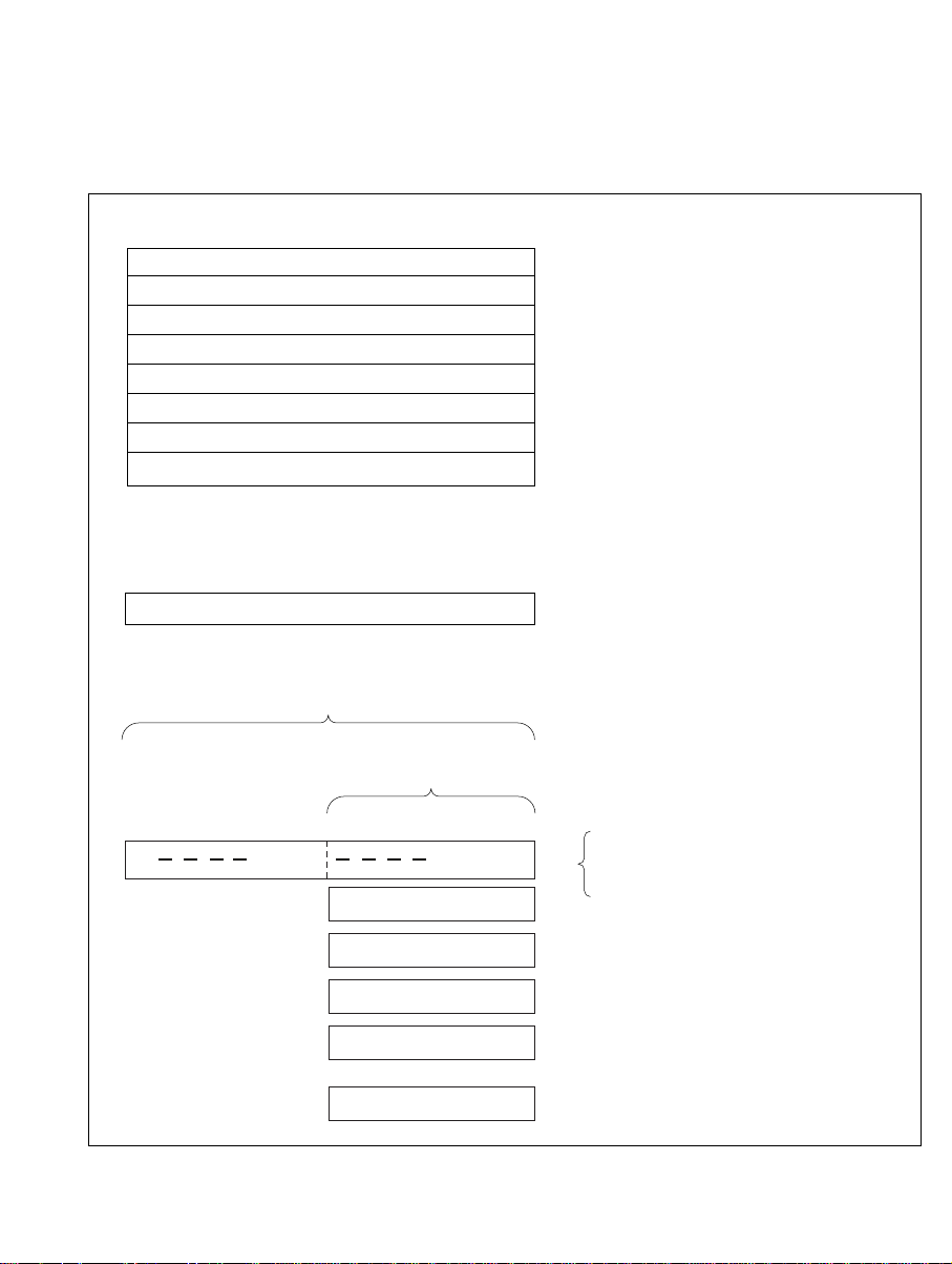
3.1.3 Register Configuration
T I2 I1 I0 NZVC
Figure 3-2 shows the register structure of the CPU. There are two groups of registers: the general
registers (Rn) and control registers (CR).
General registers (Rn)
15 0
R 0
R 1
R 2
R 3
R 4
R 5
R 6
(FP)
(SP)
R 7
Control registers (CR)
15 0
FP: Frame Pointer
SP: Stack Pointer
P C
S R
C C R
15 8 7 0
C P
D P
E P
T P
B R
Figure 3-2 Registers in the CPU
PC: Program Counter
SR: Status Register
CCR: Condition Code Register
CP: Code Page register
DP: Data Page register
EP: Extended Page register
TP: sTack Page register
BR: Base Register
33

3.2 CPU Register Descriptions
SP
Unused area
Stack area
3.2.1 General Registers
All eight of the 16-bit general registers are functionally alike; there is no distinction between data
registers and address registers. When these registers are accessed as data registers, either byte or
word size can be selected.
R6 and R7, in addition to functioning as general registers, have special assignments.
R7 is the stack pointer, used implicitly in exception handling and subroutine calls. It can be
designated by the name SP, which is synonymous with R7. As indicated in figure 3-3, it points to
the top of the stack. It is also used implicitly by the LDM and STM instructions, which load and
store multiple registers from and to the stack and pre-decrement or post-increment R7 accordingly.
R6 functions as a frame pointer (FP). The LINK and UNLK use R6 implicitly to reserve or
release a stack frame.
Figure 3-3 Stack Pointer
34

3.2.2 Control Registers
The CPU control registers (CR) include a 16-bit program counter (PC), a 16-bit status register
(SR), four 8-bit page registers, and one 8-bit base register (BR).
Program Counter (PC): This 16-bit register indicates the address of the next instruction the
CPU will execute.
Status Register (SR): This 16-bit register contains internal status information. The lower half of
the status register is referred to as the condition code register (CCR): it can be accessed as a
separate condition code byte.
CCR
Bit 1514131211109876543210
T————I2I1I0————N Z V C
Bit 15—Trace (T): When this bit is set to “1,” the CPU operates in trace mode and generates a
trace exception after every instruction. See section 4.4, “Trace” for a description of the trace
exception-handling sequence.
When the value of this bit is “0,” instructions are executed in normal continuous sequence. This
bit is cleared to “0” at a reset.
Bits 14 to 11—Reserved: These bits cannot be modified and are always read as “0.”
Bits 10 to 8—Interrupt Mask (I2, I1, I0): These bits indicate the interrupt request mask level
(0 to 7). As shown in table 3-1, an interrupt request is not accepted unless it has a higher level
than the value of the mask. A nonmaskable interrupt (NMI), which has level 8, is accepted at any
mask level. After an interrupt is accepted, I2, I1, and I0 are changed to the level of the interrupt.
Table 3-2 indicates the values of the I bits after an interrupt is accepted.
A reset sets all three of bits (I2, I1, and I0) to “1,” masking all interrupts except NMI.
35

Table 3-1 Interrupt Mask Levels
Mask Mask Bits
Priority Level I2 I1 I0 Interrupts Accepted
High 7 1 1 1 NMI
6 1 1 0 Level 7 and NMI
5 1 0 1 Levels 6 to 7 and NMI
4 1 0 0 Levels 5 to 7 and NMI
3 0 1 1 Levels 4 to 7 and NMI
2 0 1 0 Levels 3 to 7 and NMI
1 0 0 1 Levels 2 to 7 and NMI
Low 0 0 0 0 Levels 1 to 7 and NMI
Table 3-2 Interrupt Mask Bits after an Interrupt is Accepted
Level of Interrupt Accepted I2 I1 I0
NMI (8) 1 1 1
7 111
6 110
5 101
4 100
3 011
2 010
1 001
36

Bits 7 to 4—Reserved: These bits cannot be modified and are always read as “0.”
Bit 3—Negative (N): This bit indicates the most significant bit (sign bit) of the result of an
instruction.
Bit 2—Zero (Z): This bit is set to “1” to indicate a zero result and cleared to “0” to indicate a
nonzero result.
Bit 1—Overflow (V): This bit is set to “1” when an arithmetic overflow occurs, and cleared to
“0” at other times.
Bit 0—Carry (C): This bit is set to “1” when a carry or borrow occurs at the most significant bit,
and is cleared to “0” (or left unchanged) at other times.
The specific changes that occur in the condition code bits when each instruction is executed are
listed in appendix A.1 “Instruction Tables.” See the H8/500 Series Programming Manual for
further details.
Page Registers: The code page register (CP), data page register (DP), extended page register
(EP), and stack page register (TP) are 8-bit registers that are used only in the maximum mode. No
use of their contents is made in the minimum mode.
In the maximum mode, the page registers combine with the program counter and general registers
to generate 24-bit effective addresses as shown in figure 3-4, thereby expanding the program area,
data area, and stack area.
37
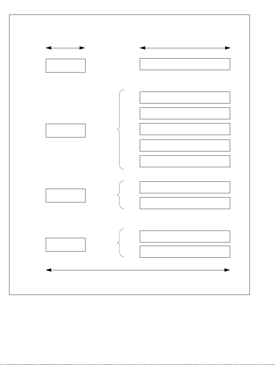
Page register
PC or general register
8 Bits 16 Bits
CP
DP
EP
TP
PC
R0
R1
R2
R3
@ aa : 16
R4
R5
R6
R7
24 Bits (effective address)
Figure 3-4 Combinations of Page Registers with Other Registers
Code Page Register (CP): The code page register and the program counter combine to generate
a 24-bit program code address. In the maximum mode, the code page register is initialized at a
reset to a value loaded from the vector table, and both the code page register and program counter
38

are saved and restored in exception handling.
Data Page Register (DP): The data page register combines with general registers R0 to R3 to
generate a 24-bit effective address. The data page register contains the upper 8 bits of the address.
It is used to calculate effective addresses in the register indirect addressing mode using R0 to R3,
and in the 16-bit absolute addressing mode (@aa:16).
The data page register is rewritten by the LDC instruction.
Extended Page Register (EP): The extended page register combines with general register R4 or
R5 to generate a 24-bit operand address. The extended page register contains the upper 8 bits of
the address. It is used to calculate effective addresses in the register indirect addressing mode
using R4 or R5.
The extended page can be used as an additional data page.
Stack Page Register (TP): The stack page register combines with R6 (FP) or R7 (SP) to
generate a 24-bit stack address. The stack page register contains the upper 8 bits of the address. It
is used to calculate effective addresses in the register indirect addressing mode using R6 or R7, in
exception handling, and subroutine calls.
Base Register (BR): This 8-bit register stores the base address used in the short absolute
addressing mode (@aa:8). In this addressing mode a 16-bit effective address in page 0 is
generated by using the contents of the base register as the upper 8 bits and an address given in the
instruction code as the lower 8 bits. See figure 3-5.
In the short absolute addressing mode the address is always located in page 0.
8 Bits 8 Bits
BR @ aa : 8
16 Bits (effective address)
Figure 3-5 Short Absolute Addressing Mode and Base Register
39

3.2.3 Initial Register Values
When the CPU is reset, its internal registers are initialized as shown in table 3-3. Note that the
stack pointer (R7) and base register (BR) are not initialized to fixed values. Also, of the page
registers used in maximum mode, only the code page register (CP) is initialized; the other three
page registers come out of the reset state with undetermined values.
Accordingly, in the minimum mode the first instruction executed after a reset should initialize the
stack pointer. The base register must also be initialized before the short absolute addressing mode
(@aa:8) is used.
In the maximum mode, the first instruction executed after a reset should initialize the stack page
register (TP) and the next instruction should initialize the stack pointer. Later instructions should
initialize the base register and the other page registers as necessary.
40

Table 3-3 Initial Values of Registers
Initial Value
Register Minimum Mode Maximum Mode
General registers
15 0 Undetermined Undetermined
R7 – R0
Control registers
15 0 Loaded from vector table Loaded from vector table
PC
SR
CCR
15 87 0 H'070x H'070x
T– – – – I2I1I0 – – – – NZVC (x: undetermined) (x: undetermined)
70
CP Undetermined Loaded from vector table
70
DP Undetermined Undetermined
70
EP Undetermined Undetermined
70
TP Undetermined Undetermined
70
BR Undetermined Undetermined
3.3 Data Formats
The H8/500 can process 1-bit data, 4-bit BCD data, 8-bit (byte) data, 16-bit (word) data, and 32bit (longword) data.
• Bit manipulation instructions operate on 1-bit data.
• Decimal arithmetic instructions operate on 4-bit BCD data.
• Almost all instructions operate on byte and word data.
• Multiply and divide instructions operate on longword data.
3.3.1 Data Formats in General Registers
Data of all the sizes above can be stored in general registers as shown in table 3-4.
41

Bit data locations are specified by bit number. Bit 15 is the most significant bit. Bit 0 is the least
significant bit. BCD and byte data are stored in the lower 8 bits of a general register. Word data
use all 16 bits of a general register. Longword data use two general registers: the upper 16 bits
are stored in Rn (n must be an even number); the lower 16 bits are stored in Rn+1.
Operations performed on BCD data or byte data do not affect the upper 8 bits of the register.
Table 3-4 General Register Data Formats
Data Type Register No. Data Structure
1-Bit
Rn
15 0
1514131211109876543210
BCD
15 87 43 0
Rn
Don’t-care Upper digit Lower digit
Byte
15 8 7 0
Rn
Don’t-care MSB LSB
Word
15 0
Rn
Longword
Rn*
MSB LSB
31 16
MSB Upper 16 bits
Rn+1*
15 0
* For longword data n must be even (0, 2, 4, or 6).
3.3.2 Data Formats in Memory
Lower 16 bits LSB
Table 3-5 indicates the data formats in memory.
Instructions that access bit data in memory have byte or word operands. The instruction specifies
a bit number to indicate a specific bit in the operand.
Access to word data in memory must always begin at an even address. Access to word data
starting at an odd address causes an address error. The upper 8 bits of word data are stored in
address n (where n is an even number); the lower 8 bits are stored in address n+1.
42

Table 3-5 Data Formats in Memory
7
6543 2107
15 14 13 12 11 10 9 8
6543210
MSB LSB
MSB
LSB
Upper 8 bits
Lower 8 bits
Address n
Even address
Odd address
Address n
Even address
Odd address
70
Data Type Data Format
1-Bit (in byte
operand data)
1-Bit (in word
operand data)
Byte
Word
When the stack is accessed in exception processing (to save or restore the program counter, code
page register, or status register), word access is always performed, regardless of the actual data
size. Similarly, when the stack is accessed by an instruction using the pre-decrement or postincrement register indirect addressing mode specifying R7 (@–R7 or @R7+), which is the stack
pointer, word access is performed regardless of the operand size specified in the instruction. An
address error will therefore occur if the stack pointer indicates an odd address. Programs should
be coded so that the stack pointer always indicates an even address.
Table 3-6 shows the data formats on the stack.
43

Table 3-6 Data Formats on the Stack
MSB
LSB
Upper 8 bits
Lower 8 bits
Even address
Odd address
Even address
Odd address M S B LSB
Don’t-care
Effective address field Effective address extension Operation code
Data Type Data Format
Byte data
on stack
Word data
on stack
3.4 Instructions
3.4.1 Basic Instruction Formats
There are two basic CPU instruction formats: the general format and the special format.
General format: This format consists of an effective address (EA) field, an effective address
extension field, and an operation code (OP) field. The effective address is placed before the
operation code because this results in faster execution of the instruction.
• Effective address field: One byte containing information used to calculate the effective
address of an operand.
• Effective address extension: Zero to two bytes containing a displacement value, immediate
data, or an absolute address. The size of the effective address
extension is specified in the effective address field.
• Operation code: Defines the operation to be carried out on the operand located at
the address calculated from the effective address information.
Some instructions (DADD, DSUB, MOVFPE, MOVTPE) have
an extended format in which the operand code is preceded by a
one-byte prefix code.
44

• (Example of prefix code in DADD instruction)
Operation code Effective address field Effective address extension
Effective address Prefix code Operation code
10100rrr 00000000 10100rrr
Special Format: In this format the operation code comes first, followed by the effective address
field and effective address extension. This format is used in branching instructions, system
control instructions, and other instructions that can be executed faster if the operation is specified
before the operand.
• Operation code: One or two bytes defining the operation to be performed by the instruction.
• Effective address field and effective address extension: Zero to three bytes containing
information used to calculate an effective address.
3.4.2 Addressing Modes
The CPU supports 7 addressing modes: (1) register direct; (2) register indirect; (3) register
indirect with displacement; (4) register indirect with pre-decrement or post-increment; (5)
immediate; (6) absolute; and (7) PC-relative.
Due to the highly orthogonal nature of the instruction set, most instructions having operands can
use any applicable addressing mode from (1) through (6). The PC-relative mode (7) is used by
branching instructions.
In most instructions, the addressing mode is specified in the effective address field. The effectiveaddress extension, if present, contains a displacement, immediate data, or an absolute address.
Table 3-7 indicates how the addressing mode is specified in the effective address field.
45
Table 3-7 Addressing Modes
No. Addressing Mode Mnemonic EA Field EA Extension
1 Register direct Rn 1 0 1 0 Sz r r r None
*1 *2
2 Register indirect @Rn 1 1 0 1 Sz r r r None
3 Register indirect @(d:8,Rn) 1 1 1 0 Sz r r r Displacement (1 byte)
with displacement
@(d:16,Rn) 1 1 1 1 Sz r r r Displacement (2 bytes)
4 Register indirect @–Rn 1 0 1 1 Sz r r r
with pre-decrement None
Register indirect @Rn+ 1 1 0 0 Sz r r r
with post-increment
5 Immediate #xx:8 0 0 0 0 0 1 0 0 Immediate data (1 byte)
#xx:16 0 0 0 0 1 1 0 0 Immediate data (2 bytes)
3
6 Absolute
*
@aa:8 0 0 0 0 Sz 1 0 1 1-Byte absolute address
(offset from BR)
@aa:16 0 0 0 1 Sz 1 0 1 2-Byte absolute address
7 PC-relative disp No EA field. 1- or 2-byte displacement
Addressing mode
is specified in the
operation code.
Notes: * 1 Sz: Specifies the operand size.
When Sz = 0: byte operand
When Sz = 1: word operand
* 2 rrr: Register number field, specifying a general register number.
0 0 0 — R0 0 0 1 — R1 0 1 0 — R2 0 1 1 — R3
1 0 0 — R4 1 0 1 — R5 1 1 0 — R6 1 1 1 — R7
* 3 The @aa:8 addressing mode is also referred to as the short absolute addressing mode.
46

3.4.3 Effective Address Calculation
Table 3-8 explains how the effective address is calculated in each addressing mode.
Table 3-8 Effective Address Calculation
No. Addressing Mode Effective Address Calculation Effective Address
1 Register direct — Operand is contents of
Rn Rn
1010Sz rrr
2 Register indirect — 23 15 0
1
@Rn DP
1101Sz rrr
3 Register indirect 8 Bits
with displacement 15 0 23 15 0
@(d:8,Rn) Rn DP
15 0 Or TP or EP
1110Sz rrr Displacement with
sign extension
+
*
Or TP or EP
1
*
2
*
2
*
Rn
Result
@(d:16,Rn) 16 Bits
1111Sz rrr 15 0 23 15 0
1
Rn DP
15 0 Or TP or EP
Displacement
+
*
2
*
Result
4 Register indirect 15 0 23 15 0
1
with pre-decrement Rn DP
@–Rn Or TP or EP
1011Sz rrr
Rn is decremented by –1 or –2
before instruction execution.
1 or 2
–
*3*4*
5
*
Result
*2
Register indirect — 23 15 0
1
with post-increment DP
*
Rn
@Rn+ Rn is incremented by +1 or +2
1100Sz rrr after instruction execution.
*3*4*
5
Or TP or EP
2
*
47
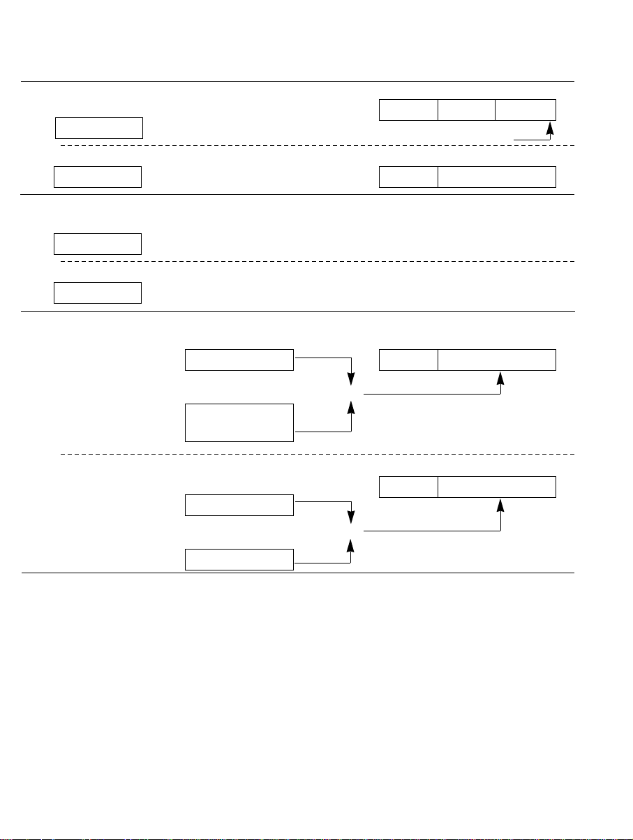
Table 3-8 Effective Address Calculation (cont)
No. Addressing Mode Effective Address Calculation Effective Address
5 Absolute address — 23 15 0
@aa:8 H'00 BR
0000Sz101 EA extension data
@aa:16 — 23 15 0
0001Sz101 DP EA extension data
6 Immediate — Operand is 1-byte EA
#xx:8 extension data.
00000100
#xx:16 — Operand is 2-byte EA
00001100 extension data.
7 PC-relative 8 Bits
disp:8 15 0 23 15 0
1
No EA code PC CP
Specified in OP code
15 0
⊕
Displacement with
sign extension
*
Result
disp:16 16 Bits 23 15 0
No EA code 15 0 CP
Specified in OP code PC
15 0
Displacement
Notes: * 1 The page register is ignored in minimum mode.
* 2 The page register used in addressing modes 2, 3, and 4 depends on the general register :
DP for R0, R1, R2, or R3; EP for R4 or R5; TP for R6 or R7.
* 3 Decrement by –1 for a byte operand, and by –2 for a word operand.
* 4 The pre-decrement or post-increment is always ±2 when R7 is specified, even if the
operand is byte size.
* 5 The drawing below shows what happens when the @-SP and @ SP+ addressing
modes are used to save and restore the stack pointer.
48
⊕
1
*
Result
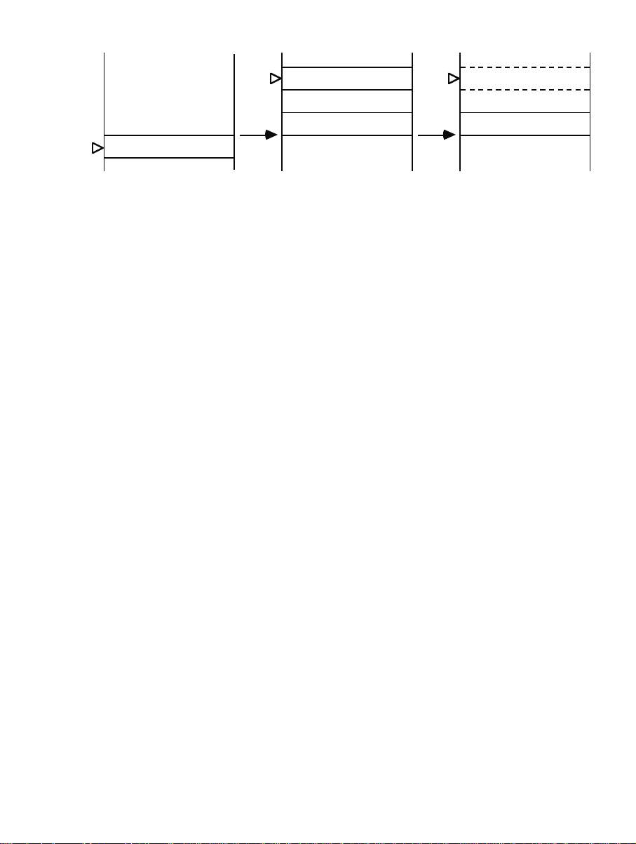
SP
Old SP-2 (upper byte)
Old SP-2 (lower byte)
MOV.W SP, @–SP MOV.W @SP+.SP
SP SP
49

3.5 Instruction Set
3.5.1 Overview
The main features of the CPU instruction set are:
• A general-register architecture.
• Orthogonality. Addressing modes and data sizes can be specified independently in each instruction.
• 1.5 addressing modes (supporting register-register and register-memory operations)
• Affinity for high-level languages, particularly C, with short formats for frequently-used
instructions and addressing modes.
• Standard mnemonics, common throughout the H Series.
The CPU instruction set includes 63 types of instructions, listed by function in table 3-9.
Table 3-9 Instruction Classification
Function Instructions Types
Data transfer MOV, LDM, STM, XCH, SWAP, MOVTPE, MOVFPE 7
Arithmetic operations ADD, SUB, ADDS, SUBS, ADDX, SUBX, DADD, DSUB, 17
MULXU, DIVXU, CMP, EXTS, EXTU, TST, NEG, CLR,
TAS
Logic operations AND, OR, XOR, NOT 4
Shift SHAL, SHAR, SHLL, SHLR, ROTL, ROTR, ROTXL, 8
ROTXR
Bit manipulation BSET, BCLR, BTST, BNOT 4
Branch Bcc*, JMP, PJMP, BSR, JSR, PJSR, RTS, PRTD, 11
PRTS, RTD, SCB (/F, /NE, /EQ)
System control TRAPA, TRAP/VS, RTE, SLEEP, LDC, STC, ANDC, 12
ORC, XORC, NOP, LINK, UNLK
Total 63
* Bcc is a conditional branch instruction in which cc represents a condition code.
Tables 3-10 to 3-16 give a concise summary of the instructions in each functional category. The
MOV, ADD, and CMP instructions have special short formats, which are listed in table 3-17. For
detailed descriptions of the instructions, refer to the H8/500 Series Programming Manual.
The notation used in tables 3-10 to 3-17 is defined below.
50

Operation Notation
Rd General register (destination)
Rs General register (source)
Rn General register
(EAd) Destination operand
(EAs) Source operand
CCR Condition code register
N N (negative) bit of CCR
Z Z (zero) bit of CCR
V V (overflow) bit of CCR
C C (carry) bit of CCR
CR Control register
PC Program counter
CP Code page register
SP Stack pointer
FP Frame pointer
#IMM Immediate data
disp Displacement
+ Addition
– Subtraction
× Multiplication
÷ Division
∧ AND logical
∨ OR logical
⊕ Exclusive OR logical
→ Move
↔ Exchange
¬ Not
51

3.5.2 Data Transfer Instructions
Table 3-10 describes the seven data transfer instructions.
Table 3-10 Data Transfer Instructions
Instruction Size* Function
Data MOV (EAs) → (EAd), #IMM → (EAd)
transfer MOV:G B/W Moves data between two general registers, or between
MOV:E B a general register and memory, or moves immediate data
MOV:I W to a general register or memory.
MOV:F B/W
MOV:L B/W
MOV:S B/W
LDM W Stack → Rn (register list)
Pops data from the stack to one or more registers.
STM W Rn (register list) → stack
Pushes data from one or more registers onto the stack.
XCH W Rs ↔ Rd
Exchanges data between two general registers.
SWAP B Rd (upper byte) ↔ Rd (lower byte)
Exchanges the upper and lower bytes in a general register.
MOVTPE B Rn → (EAd)
Transfers data from a general register to memory in
synchronization with the E clock.
MOVFPE B (EAs) → Rd
Transfers data from memory to a general register in
synchronization with the E clock.
Note: B—byte; W—word
52

3.5.3 Arithmetic Instructions
Table 3-11 describes the 17 arithmetic instructions.
Table 3-11 Arithmetic Instructions
Instruction Size Function
Arithmetic ADD Rd ± (EAs) → Rd, (EAd) ± #IMM → (EAd)
operations ADD:G B/W Performs addition or subtraction on data in a general
ADD:Q B/W register and data in another general register or memory, or
SUB B/W on immediate data and data in a general register or memory.
ADDS B/W
SUBS B/W
ADDX B/W Rd ± (EAs) ± C → Rd
SUBX B/W Performs addition or subtraction with carry or borrow on
data in a general register and data in another general
register or memory, or on immediate data and data in a
general register or memory.
DADD B (Rd)
DSUB B Performs decimal addition or subtraction on data in two
MULXU B/W Rd × (EAs) → Rd
DIVXU B/W Rd ÷ (EAs) → Rd
CMP Rn – (EAs), (EAd) – #IMM
CMP:G B/W Compares data in a general register with data in another
CMP:E B general register or memory, or with immediate data, or
CMP:I W compares immediate data with data in memory.
Note: B—byte; W—word
10 ± (Rs)10 ±C → (Rd)10
general registers.
Performs 8-bit × 8-bit or 16-bit × 16-bit unsigned
multiplication on data in a general register and data in
another general register or memory, or on data in a
general register and immediate data.
Performs 16-bit ÷ 8-bit or 32-bit ÷ 16-bit unsigned division
on data in a general register and data in another general
register or memory, or on data in a general register and
immediate data.
53

Table 3-11 Arithmetic Instructions (cont)
Instruction Size Function
Arithmetic EXTS B (<bit 7> of <Rd>) → (<bits 15 to 8> of <Rd>)
operations Converts byte data in a general register to word data by
extending the sign bit.
EXTU B 0 → (<bits 15 to 8> of <Rd>)
Converts byte data in a general register to word data by
padding with zero bits.
TST B/W (EAd) – 0
Compares general register or memory contents with 0.
NEG B/W 0 – (EAd) → (EAd)
Obtains the two’s complement of general register or
memory contents.
CLR B/W 0 → (EAd)
Clears general register or memory contents to 0.
TAS B (EAd) — 0, (1)
Tests general register or memory contents, then sets the
most significant bit (bit 7) to “1.”
Note: B—byte; W—word
2 → (<bit 7> of <EAd>)
3.5.4 Logic Operations
Table 3-12 lists the four instructions that perform logic operations.
Table 3-12 Logic Operation Instructions
Instruction Size Function
Logical AND B/W Rd∧(EAs) → Rd
operations Performs a logical AND operation on a general register
and another general register, memory, or immediate data.
OR B/W Rd∨(EAs) → Rd
Performs a logical OR operation on a general register and
another general register, memory, or immediate data.
XOR B/W Rd⊕(EAs) → Rd
Performs a logical exclusive OR operation on a general register
and another general register, memory, or immediate data.
NOT B/W ¬ (EAd) → (EAd)
Obtains the one’s complement of general register or memory
contents.
Note: B—byte; W—word
54

3.5.5 Shift Operations
Table 3-13 lists the eight shift instructions.
Table 3-13 Shift Instructions
Instruction Size Function
Shift SHAL B/W (EAd) shift → (EAd)
operations SHAR B/W Performs an arithmetic shift operation on general register
or memory contents.
SHLL B/W (EAd) shift → (EAd)
SHLR B/W Performs a logical shift operation on general register or
memory contents.
ROTL B/W (EAd) shift → (EAd)
ROTR B/W Rotates general register or memory contents.
ROTXL B/W (EAd) rotate through carry → (EAd)
ROTXR B/W Rotates general register or memory contents through the
C (carry) bit.
Note: B—byte; W—word
55

3.5.6 Bit Manipulations
Table 3-14 describes the four bit-manipulation instructions.
Table 3-14 Bit-Manipulation Instructions
Instruction Size Function
Bit BSET B/W ¬ (<bit-No.> of <EAd>) → Z,
manipu- 1 → (<bit-No.> of <EAd>)
lations Tests a specified bit in a general register or memory, then
sets the bit to “1.” The bit is specified by a bit number
given in immediate data or a general register.
BCLR B/W ¬ (<bit-No.> of <EAd>) → Z,
0 → (<bit-No.> of <EAd>)
Tests a specified bit in a general register or memory, then
clears the bit to “0.” The bit is specified by a bit number
given in immediate data or a general register.
BNOT B/W ¬ (<bit-No.> of <EAd>) → Z,
→ (<bit-No.> of <EAd>)
Tests a specified bit in a general register or memory, then
inverts the bit. The bit is specified by a bit number given
in immediate data or a general register.
BTST B/W ¬ (<bit-No.> of <EAd>) → Z
Tests a specified bit in a general register or memory. The
bit is specified by a bit number given in immediate data or
a general register.
Note: B—byte; W—word
56

3.5.7 Branching Instructions
Table 3-15 describes the 11 branching instructions.
Table 3-15 Branching Instructions
Instruction Size Function
Branch Bcc — Branches if condition cc is true.
Mnemonic Description Condition
BRA (BT) Always (true) True
BRN (BF) Never (false) False
BHI High C ∨ Z = 0
BLS Low or Same C ∨ Z = 1
BCC (BHS) Carry Clear C = 0
(High or Same)
BCS (BLO) Carry Set (Low) C = 1
BNE Not Equal Z = 0
BEQ Equal Z = 1
BVC Overflow Clear V = 0
BVS Overflow Set V = 1
BPL Plus N = 0
BMI Minus N = 1
BGE Greater or Equal N ⊕ V = 0
BLT Less Than N ⊕ V = 1
BGT Greater Than Z ∨ (N ⊕ V) = 0
BLE Less or Equal Z ∨ (N ⊕ V) = 1
JMP — Branches unconditionally to a specified address in the same page.
PJMP — Branches unconditionally to a specified address in a specified page.
BSR — Branches to a subroutine at a specified address in the same page.
JSR — Branches to a subroutine at a specified address in the same page.
PJSR — Branches to a subroutine at a specified address in a specified page.
RTS — Returns from a subroutine in the same page.
57

Table 3-15 Branching Instructions (cont)
Instruction Size Function
Branch PRTS — Returns from a subroutine in a different page.
RTD — Returns from a subroutine in the same page and adjusts
the stack pointer.
PRTD — Returns from a subroutine in a different page and adjusts
the stack pointer.
SCB/F — Controls a loop using a loop counter and/or a specified
SCB/NE — termination condition.
SCB/EQ —
58

3.5.8 System Control Instructions
Table 3-16 describes the 12 system control instructions.
Table 3-16 System Control Instructions
Instruction Size Function
System TRAPA — Generates a trap exception with a specified vector number.
control TRAP/VS — Generates a trap exception if the V bit is set to “1” when
the instruction is executed.
RTE — Returns from an exception-handling routine.
LINK — FP → @–SP; SP → FP; SP + #IMM → SP
Creates a stack frame.
UNLK — FP → SP; @SP+ → FP
Deallocates a stack frame created by the LINK instruction.
SLEEP — Causes a transition to the power-down state.
LDC B/W* (EAs) → CR
Moves immediate data or general register or memory
contents to a specified control register.
STC B/W* CR → (EAd)
Moves control register data to a specified general register
or memory location.
ANDC B/W* CR ∧ #IMM → CR
Logically ANDs a control register with immediate data.
ORC B/W* CR ∨ #IMM → CR
Logically ORs a control register with immediate data.
XORC B/W* CR ⊕ #IMM → CR
Logically exclusive-ORs a control register with immediate
data.
NOP — PC + 1 → PC
No operation. Only increments the program counter.
* The size depends on the control register.
When using the LDC and STC instructions to stack and unstack the BR, CCR, TP, DP, and EP
control registers in the H8/500 family, note the following point.
H8/500 hardware does not permit byte access to the stack. If the LDC.B or STC.B assembler
mnemonic is coded with the @R7 + (@SP+) or @–R7 (@–SP) addressing mode, the stackpointer addressing mode takes precedence and hardware automatically performs word access.
59

Specifically, the LDC.B and STC.B instructions are executed as follows.
EP
a
DP
b
Old SP – 2
Before execution
Old SP – 1
Old SP
New SP
After execution
New SP + 1
New SP + 2
a
b
EP
a
DP
b
Old SP
After execution
Old SP + 1
Old SP + 2
New SP – 2
Before execution
New SP – 1
New SP
a
b
EP
a
DP
b
CCR
a
Old SP – 2
Before execution
Old SP – 1
Old SP
New SP
After execution
New SP + 1
New SP + 2
a
b
The following applies only to the stack-pointer addressing modes. In addressing modes that do not
use the stack pointer, byte data access is performed as specified by the assembler mnemonic.
(1) STC.B EP, @–SP
When word data access is applied to EP, both EP and DP are accessed. This instruction
stores EP at address SP (old) –2, and DP at address SP (old) –1.
(2) LDC.B @SP+, EP
When word data access is applied to EP, both EP and DP are accessed. This instruction
loads EP from address SP (old), and DP from address SP (old) +1, updating the DP value as
well as the EP value.
(3) STC.B CCR, @–SP
When word data access is applied to CCR, only CCR is accessed. This instruction stores
identical CCR contents at both address SP (old) –2 and address SP (old) –1.
60
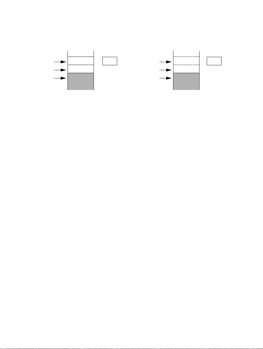
(4) LDC.B @SP+, CCR
CCR
Old SP
After execution
Old SP + 1
Old SP + 2
New SP – 2
Before execution
New SP – 1
New SP
a
b
CCR
b
When word data access is applied to CCR, only CCR is accessed. This instruction loads
CCR from address SP (old) +1. Note that the value in address SP (old) is not loaded.
BR, DP, and TP are accessed in the same way as CCR. When DP is specified, both EP and
DP are accessed, but when CCR, BR, DP, or TP is specified, only the specified register is
accessed.
61

3.5.9 Short-Format Instructions
The ADD, CMP, and MOV instructions have special short formats. Table 3-17 lists these short
formats together with the equivalent general formats.
The short formats are a byte shorter than the corresponding general formats, and most of them
execute one state faster.
Table 3-17 Short-Format Instructions and Equivalent General Formats
Short-Format Execution Equivalent General- Execution
2
Instruction Length States
1
ADD:Q #xx,Rd
CMP:E #xx:8,Rd 22 CMP:G.B #xx:8,Rd 33
CMP:I #xx:16,Rd 33 CMP:G.W #xx:16,Rd 44
MOV:E #xx:8,Rd 22 MOV:G.B #xx:8,Rd 33
MOV:I #xx:16,Rd 33 MOV:G.W #xx:16,Rd 44
MOV:L @aa:8,Rd 25 MOV:G @aa:8,Rd 35
MOV:S Rs,@aa:8 25 MOV:G Rs,@aa:8 35
MOV:F @(d:8,R6),Rd 25 MOV:G @(d:8,R6),Rd 35
MOV:F Rs,@(d:8,R6) 25 MOV:G Rs,@(d:8,R6) 35
Notes: * 1 The ADD:Q instruction accepts other destination operands in addition to a general
* 2 Number of execution states for access to on-chip memory.
*
register, but the immediate data value (#xx) is limited to ±1 or ±2.
22 ADD:G #xx:8,Rd 33
*
Format Instruction Length States
2
*
3.6 Operating Modes
The CPU operates in one of two modes: the minimum mode or the maximum mode.
These modes are selected by the mode pins (MD2 to MD0 ).
3.6.1 Minimum Mode
The minimum mode supports a maximum address space of 64k bytes. The page registers are
ignored. Instructions that branch across page boundaries (PJMP, PJSR, PRTS, PRTD) are invalid.
62

3.6.2 Maximum Mode
In the maximum mode the page registers are valid, expanding the maximum address space to 1M
byte.
The address space is divided into 64k-byte pages. The pages are separate; it is not possible to
move continuously across a page boundary.
It is possible to move from one page to another with branching instructions (PJMP, PJSR, PRTS,
PRTD). The TRAPA instruction and branches to interrupt-handling routines can also jump across
page boundaries. It is not necessary for a program to be contained in a single 64k-byte page.
When data access crosses a page boundary, the program must rewrite the page register before it
can access the data in the next page.
For further information on the operating modes, see section 2, “MCU Operating Modes and
Address Space.”
3.7 Basic Operational Timing
3.7.1 Overview
The CPU operates on a system clock (ø) which is created by dividing an oscillator frequency
(fosc) by two. One period of the system clock is referred to as a “state.” The CPU accesses
memory in a cycle consisting of 2 or 3 states. The CPU uses different methods to access on-chip
memory, the on-chip register field, and external devices.
Access to On-Chip Memory (RAM, ROM): For maximum speed, access to on-chip memory
(RAM, ROM) is performed in two states, using a 16-bit-wide data bus.
Figure 3-6 shows the on-chip memory access cycle. Figure 3-7 indicates the pin states. The bus
control signals output from the H8/532 chip go to the nonactive state during the access.
Access to On-Chip Register Field (Addresses H'FF80 to H'FFFF): The access cycle consists
of three states. The data bus is 8 bits wide.
Figure 3-8 shows the on-chip supporting module access cycle. Figure 3-9 indicates the pin states.
63
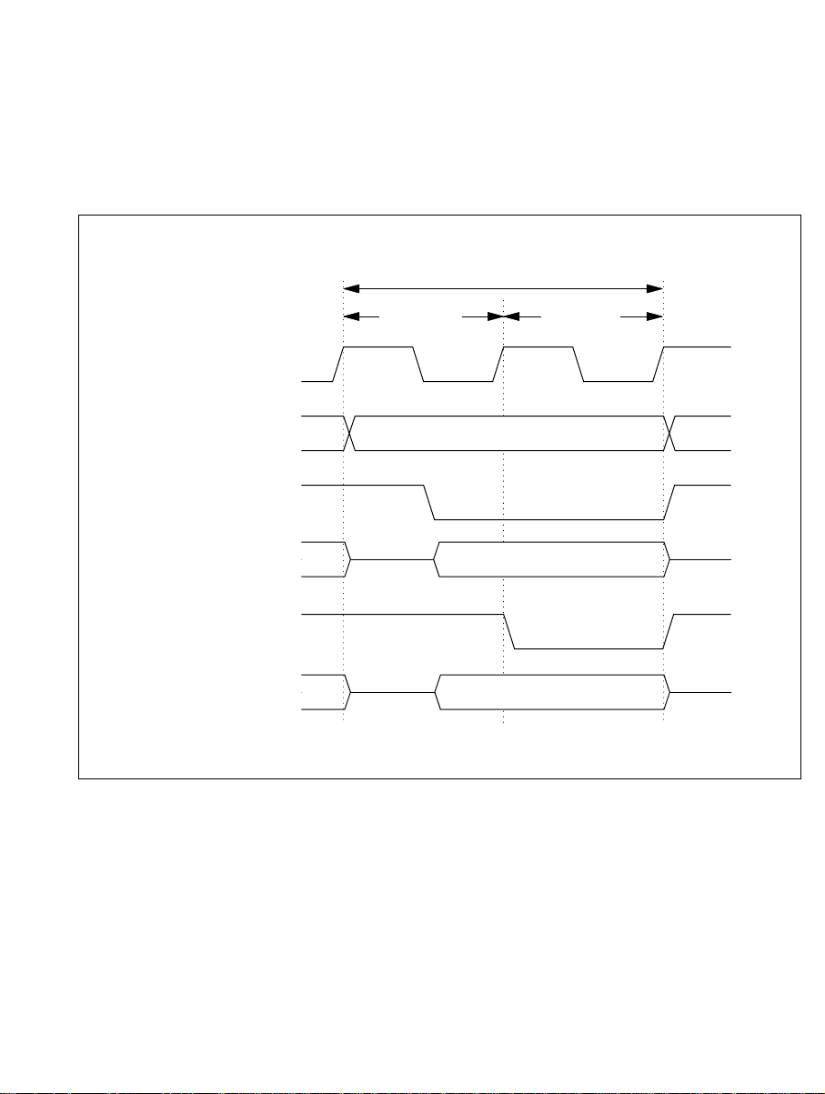
Access to External Devices: The access cycle consists of three states. The data bus is 8 bits
T state
Memory cycle
1 T state2
ø
Internal address bus
Internal Read signal
Internal data bus
(Read access)
Internal Write signal
Read data
Address
Write data
Internal data bus
(Write access)
wide. Figure 3-10 (a) and (b) shows the external access cycle. Additional wait states (Tw) can be
inserted by the wait-state controller (WSC).
3.7.2 On-Chip Memory Access Cycle
Figure 3-6 On-Chip Memory Access Timing
64
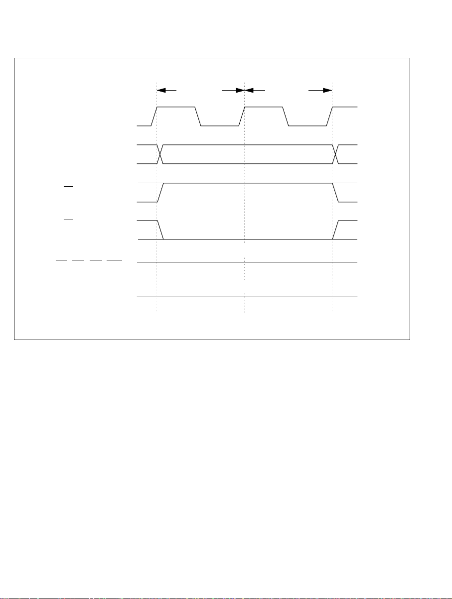
3.7.3 Pin States during On-Chip Memory Access
T state1 T state2
ø
A to A
R/W (write access)
19 0
AS, DS, RD, WR
D to D 70
R/W (read access)
“High”
High-impedance
Figure 3-7 Pin States during Access to On-Chip Memory
65
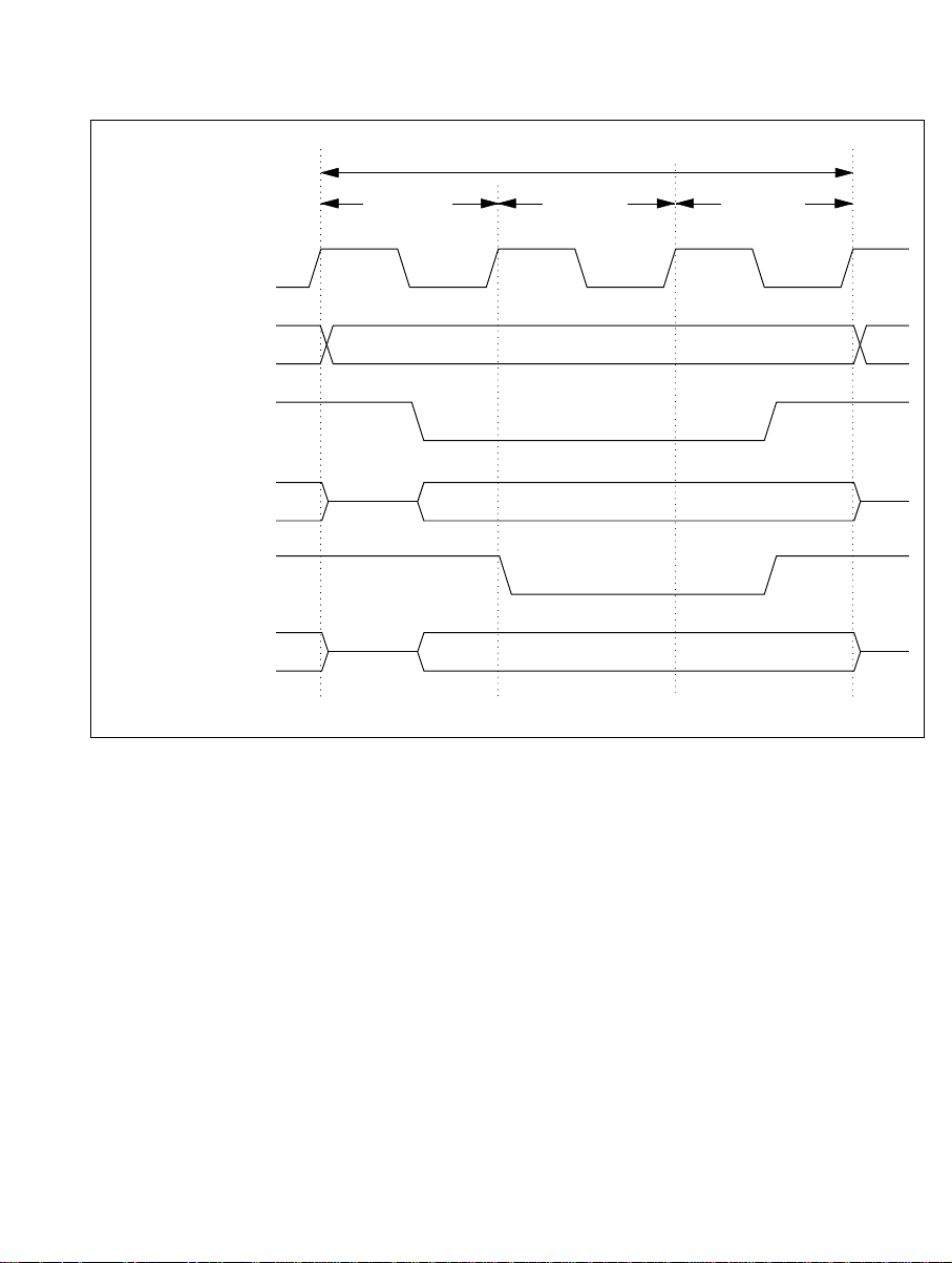
3.7.4 Register Field Access Cycle (Addresses H'FF80 to H'FFFF)
T state
Memory cycle
1 T state2 T state3
Address
Read data
ø
Internal address bus
Internal Read signal
Internal Write signal
Internal data bus
(write access)
Internal data bus
(read access)
Write data
Figure 3-8 Register Field Access Timing
66
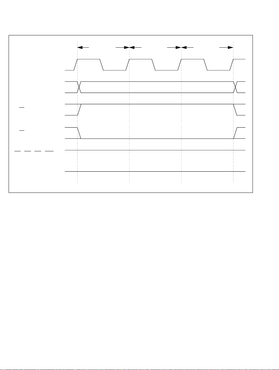
3.7.5 Pin States during Register Field Access (Addresses H'FF80 to H'FFFF)
T state1 T state2 T state3
“High”
ø
A to A
R/W (read access)
19 0
AS, DS, RD, WR
D to D 70
R/W (write access)
High-impedance
Figure 3-9 Pin States during Register Field Access
67
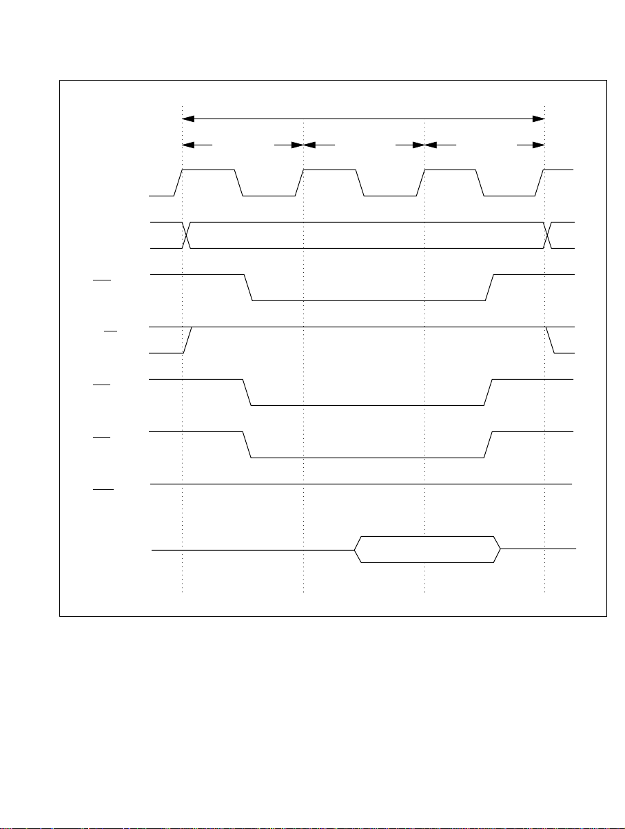
3.7.6 External Access Cycle
Read cycle
T state
1 T state2 T state3
Address
R/W
D –D70
A –A19 0
ø
AS
WR
DS
RD
“High”
Read data
Figure 3-10 (a) External Access Cycle (Read Access)
68
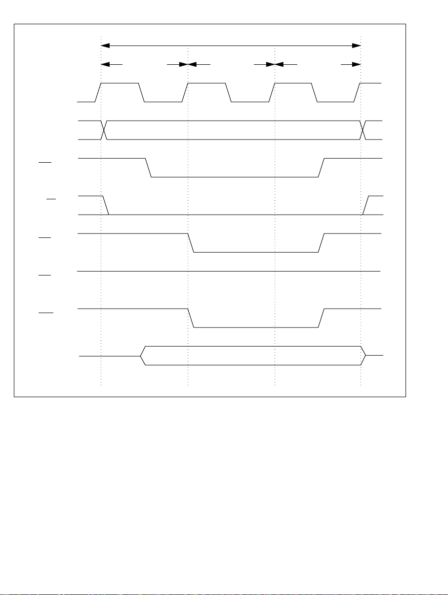
Write cycle
T state
1 T state2 T state3
Address
Write data
“High”
R/W
D –D70
A –A19 0
ø
AS
WR
DS
RD
3.8 CPU States
3.8.1 Overview
Figure 3-10 (b) External Access Cycle (Write Access)
The CPU has five states: the program execution state, exception-handling state, bus-released state,
reset state, and power-down state. The power-down state is further divided into the sleep mode,
software standby mode, and hardware standby mode. Figure 3-11 summarizes these states, and
figure 3-12 shows a map of the state transitions.
69
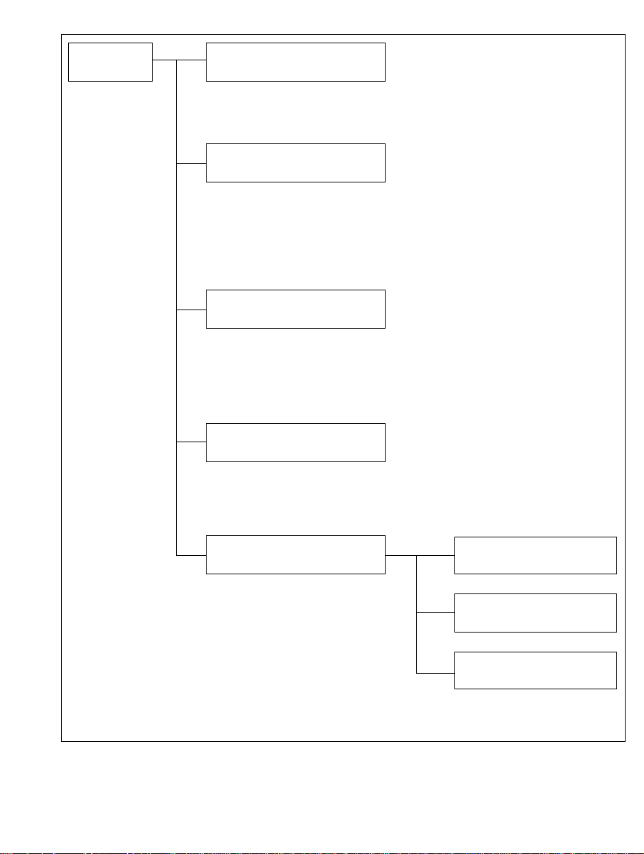
State Program execution state
The CPU executes program instructions in sequence.
Exception-handling state
A transient state in which the CPU executes a hardware
sequence (saving the program counter and status register,
fetching a vector from the vector table, etc.) triggered by a reset,
interrupt, or other exception.
Bus-released state
The state in which the CPU has released the external bus in
response to a bus request signal from an external device, and
is waiting for the bus to be returned.
Reset state
The state in which the CPU and all on-chip supporting
modules have been initialized and are stopped.
Power-down state
A state in which some
or all of the clock
signals are stopped to
conserve power.
Sleep mode
Software standby mode
Hardware standby mode
Figure 3-11 Operating States
70

BREQ = “0”
BREQ = “0”
BREQ = “1”
Bus-released state
End of
exception
handling
Request
for exception
handling
SLEEP
instruction
with standby
flag set
SLEEP
instruction
Interrupt request
NMI
Program execution state
Exception-handling
state
Sleep mode
Software standby mode
Hardware standby mode
Reset state
*
STBY = “1”, RES = “0”
RES = “1”
* From any state except the hardware standby mode, a transition to the reset state occurs
whenever RES goes Low.
* A transition to the hardware standby mode from any state occurs when STBY goes Low.
BREQ = “1”
1 *2
1
2
3.8.2 Program Execution State
In this state the CPU executes program instructions in normal sequence.
Figure 3-12 State Transitions
3.8.3 Exception-Handling State
The exception-handling state is a transient state that occurs when the CPU alters the normal
program flow due to an interrupt, trap instruction, address error, or other exception. In this state
the CPU carries out a hardware-controlled sequence that prepares it to execute a user-coded
exception-handling routine.
71

In the hardware exception-handling sequence the CPU does the following:
1. Saves the program counter and status register (in minimum mode) or program counter, code
page register, and status register (in maximum mode) to the stack.
2. Clears the T bit in the status register to “0.”
3. Fetches the start address of the exception-handling routine from the exception vector table.
4. Branches to that address, returning to the program execution state.
See section 4, “Exception Handling,” for further information on the exception-handling state.
3.8.4 Bus-Released State
When so requested, the CPU can grant control of the external bus to an external device. While an
external device has the bus right, the CPU is said to be in the bus-released state. The bus right is
controlled by two pins:
• BREQ: Input pin for the Bus Request signal from an external device
• BACK: Output pin for the Bus Request Acknowledge signal from the CPU, indicating that the
CPU has released the bus
The procedure by which the CPU enters and leaves the bus-released state is:
1. The CPU receives a Low BREQ signal from an external device.
2. The CPU places the address bus pins (A19 – A0), data bus pins (D7 – D0) and bus control pins
(RD, WR, R/W, DS, and AS) in the high-impedance state, sets the BACK pin to the Low level
to indicate that it has released the bus, then halts.
3. The external device that requested the bus (with the BREQ signal) becomes the bus master. It
can use the data bus and address bus. The external device is responsible for manipulating the
bus control signals (RD, WR, R/W, DS, and AS).
4. When the external device finishes using the bus, it clears the BREQ signal to the High level.
The CPU then reassumes control of the bus and returns to the program execution state.
Bus Release Timing: The CPU can release the bus right at the following times:
1. The BREQ signal is sampled during every memory access cycle (instruction prefetch or data
read/write). If BREQ is Low, the CPU releases the bus right at the end of the cycle. (In
word data access to external memory or an address from H'FF80 to H'FFFF, the CPU does
not release the bus right until it has accessed both the upper and lower data bytes.)
2. During execution of the MULXU and DIVXU instructions, since considerable time may
pass without an instruction prefetch or data read/write, BREQ is also sampled at internal
machine cycles, and the bus right is released if BREQ is Low.
3. The bus right can also be released in the sleep mode.
The CPU does not recognize interrupts while the bus is released.
72

Timing Charts: Timing charts of the operation by which the bus is released are shown in
RD, WR, R/W
DS, AS
D –D70
A –A19 0
ø
BREQ
BACK
On-chip memory
Access cycle
Bus-right release cycle CPU cycle
T
2 T1 T2 TX TX TX TX T1***
(1) (2) (3) (4) (5)
Fig. 3-13
figure 3-13 for the case of bus release during an on-chip memory read cycle, in figure 3-14 for
bus release during an external memory read cycle, and in figure 3-15 for bus release while the
CPU is performing an internal operation.
(1) The BREQ pin is sampled at the start of the T1 state and the Low level is detected.
(2) At the end of the memory access cycle, the BACK pin goes Low and the CPU releases the bus.
(3) While the bus is released, the BREQ pin is sampled at each Tx state.
(4) A High level is detected at the BREQ pin.
(5) The BACK pin is returned to the High level, ending the bus-right release cycle.
* T
1 and T2: On-chip memory access states.
Tx : Bus-right released state.
Figure 3-13 Bus-Right Release Cycle (During On-Chip Memory Access Cycle)
73

RD, WR
R/W, DS
D –D
70
A –A19 0
ø
BREQ
BACK
(1) (2) (3) (4)
Fig. 3-14
Bus-right release cycle CPU cycleExternal access cycle
T
1 T2 TW TXT3 TX TX T1**
(1) The BREQ pin is sampled at the start of the TW state and the Low level is detected.
(2) At the end of the external access cycle, the BA CK pin goes Lo w and the CPU releases the bus.
(3) The BREQ pin is sampled at the T
X state and a High level is detected.
(4) The BACK pin is returned to the High level, ending the bus-right release cycle.
* T
W : Wait state.
X : Bus-right released state.
T
Figure 3-14 Bus-Right Release Cycle (During External Access Cycle)
74

RD, WR
R/W, DS
D –D
70
A –A19 0
ø
BREQ
BACK
Bus-right release cycle CPU cycleExternal access cycle
Ti Ti Ti TX TX T1** TXTi
Fig. 3-15
(1) (2) (3) (4)
(1) The BREQ pin is sampled at the start of a TI state and the Low level is detected.
(2) At the end of the internal operation cycle, the BACK pin goes Lo w and the CPU releases the b us.
(3) The BREQ pin is sampled at the T
X state and a High level is detected.
(4) The BACK pin is returned to the High level, ending the bus-right release cycle.
* T
I : Internal CPU operation state.
T
X : Bus-right released state.
Figure 3-15 Bus-Right Release Cycle (During Internal CPU Operation)
75

Notes: The BREQ signal must be held Low until BACK goes Low. If BREQ returns to the High
level before BACK goes Low, the bus release operation may be executed incorrectly.
To leave the bus-released state, the High level at the BREQ pin must be sampled two times. If the
BREQ returns to Low before it is sampled two times, the bus released cycle will not end.
The bus release operation is enabled only when the BRLE bit in the port 1 control register (P1CR)
is set to “1.” When this bit is cleared to “0” (its initial value), the BREQ and BACK pins are used
for general-purpose input and output, as P13 and P12.
An instruction that sets the BRLE bit is: BSET.B #3, @H'FFFC
Note the following point when using the H8/532’s release function.
If the BREQ signal is asserted and an interrupt is requested simultaneously during execution of the
SLEEP instruction, the BACK signal may fail to be output even though the CPU has released the
bus. This may cause the system to stop for the interval during which BREQ is asserted, with no
device in control of the bus. The interrupts that can cause this state include NMI, IRQ, and all the
interrupts from on-chip supporting modules. When the BREQ signal is deasserted, ending this
state, the CPU takes control of the bus again and resumes normal instruction execution.
The following methods can be used to avoid entering this state.
Method 1: If the BREQ signal is used, do not use the SLEEP instruction.
Method 2: Disable the BREQ signal during execution of the SLEEP instruction. This can be
done by clearing the bus release enable bit (BRLE) in the port 1 control register (P1CR) to 0
immediately bifore executing the SLEEP instruction. (When the BRLE bit is cleared, low inputs
on the BREQ line are not latched on-chip.) Place instructions to set the BRLE bit to 1 at the
beginning of interrupt-handling routines. If the data transfer controller (DTC) is used, place an
instruction to set the BRLE bit immediately after the SLEEP instruction.
If method 2 is used, BREQ inputs will be ignored while the chip is in sleep mode.
(Coding example)
Main Program Interrupt-Handling Routine
BSET.B #3, @P1CR
BCLR.B #3, @P1CR
SLEEP
BSET.B #3, @P1CR RTE
76

3.8.5 Reset State
In the reset state, the CPU and all on-chip supporting modules are initialized and placed in the
stopped state. The CPU enters the reset state whenever the RES pin goes Low, unless the CPU is
currently in the hardware standby mode. It remains in the reset state until the RES pin goes High.
See section 4.2, “Reset,” for further information on the reset state.
3.8.6 Power-Down State
The power-down state comprises three modes: the sleep mode, the software standby mode, and
the hardware standby mode.
See section 18, “Power-Down State,” for further information.
77
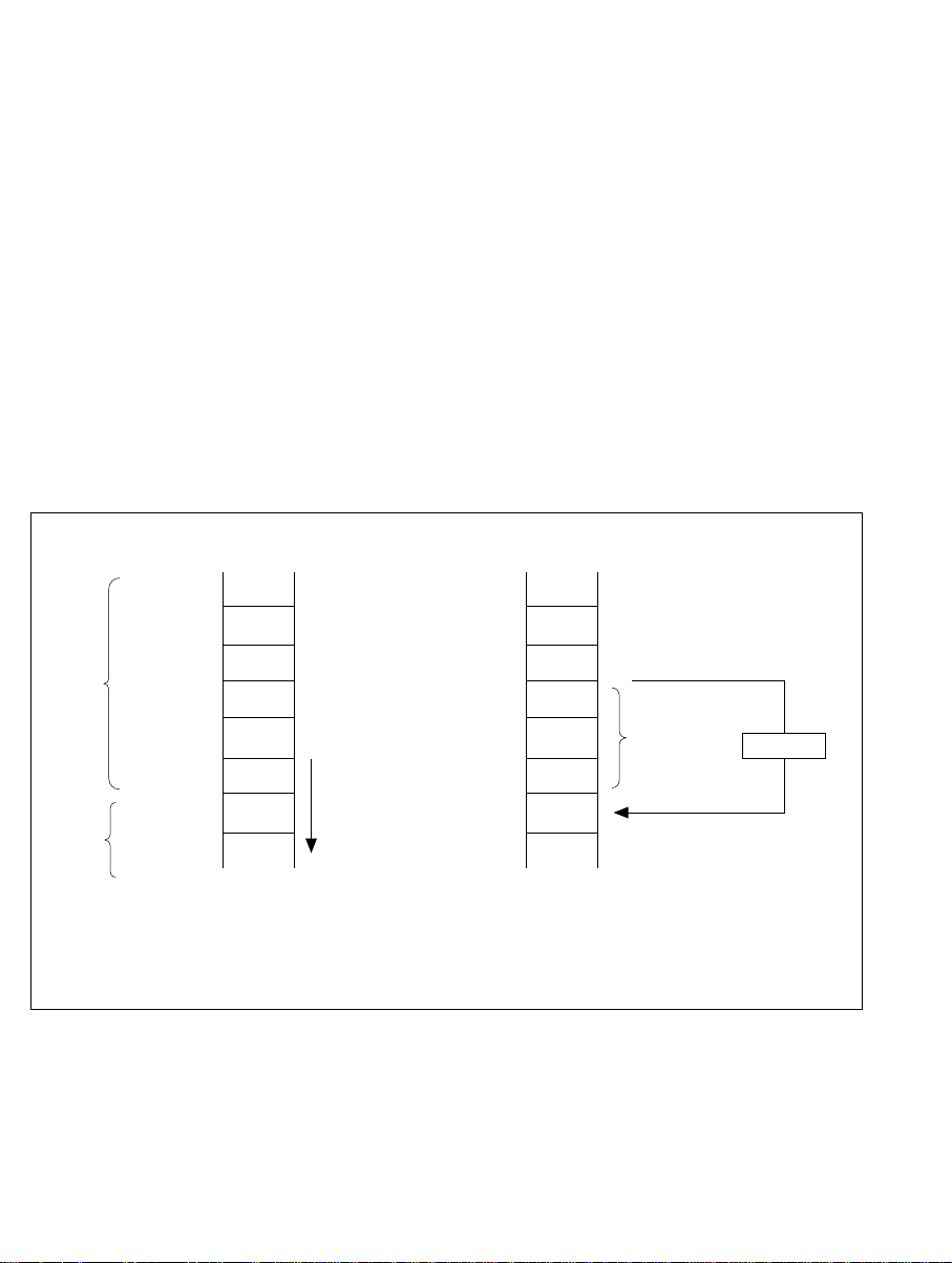
3.9 Programming Notes
H'FB7A
H'FB7B
H'FB7C
H'FB7D
H'FB7E
H'FB7F
H'FB80
H'FB81
NOP
NOP
NOP
NOP
NOP
NOP
NOP
NOP
NOP
BRA
disp
NOP
NOP
Not
executable
Do not
place
instruction
code here
Branch
H'FB7A
H'FB7B
H'FB7C
H'FB7D
H'FB7E
H'FB7F
H'FB80
H'FB81
Execution Disabled Execution Enabled
3.9.1 Restriction on Address Location
The following restriction applies when instructions are located in on-chip RAM.
• Restriction
Instruction execution cannot proceed continuously from an external address to on-chip RAM in
the ZTAT versions. This restriction does not apply to versions with masked ROM.
• Solution
To execute instructions located in on-chip RAM, use a branch instruction (examples: Bcc, JMP,
etc.) to branch to the first instruction located in on-chip RAM. Do not place instruction code in
the last three bytes of external memory (H'FB7D to H'FB7F).
78

3.9.2 Note on MULXU Instruction
Note that in the case described below, the H8/532 multiply instruction does not give correct
results.
(1) Problem
The result of a squaring operation such as MULXU.B Rn, Rn is indeterminate. This problem
occurs when the same register is specified for the source and destination of a byte
multiplication operation.
This problem occurs only in ZTAT versions of the H8/532. It does not occur in versions
with masked ROM.
(2) Solution
The problem can be avoided by the following methods.
➀ Place the source and destination operands in different registers.
Example: MULXU.B R4, R4 → MOV.W R4, R5
MULXU.B R5, R4
➁ Use a word multiplication instruction.
Example: MULXU.B R4, R4 → MULXU.W R4, R4
MOV.W R5, R4
➂ Place one of the operands in memory.
Example: MULXU.B R4, R4 → MOV.W R4, @–SP
MULXU.B @(1,SP), R4
ADDS #2, SP
This problem occurs only in the H8/532. It does not occur in other chips in the H8/500
Series (such as the H8/520).
(3) Note on usage of C compiler
Programmers using the C compiler should bear the following programming note in mind.
• Conditions under which the compiler generates a MULXU.B Rn, Rn instruction
The C compiler generates a MULXU.B Rn, Rn instruction when the following two conditions
are satisfied in the source program:
79

➀ A one-byte variable (char or unsigned char) is declared as a register variable.
➁ The variable declared as in ➀ is squared by compound substitution
Example: register char a;
a *= a;
• Solution
The problem can be avoided as follows:
➀ In the example above, do not declare the variable (a) as a register variable.
Example: register char a; → char a;
a *= a; a *= a;
➁ When squaring one-byte data, do not use compound substitution. Code as follows:
Example: a *= a; → a = a *a;
80

Section 4 Exception Handling
4.1 Overview
4.1.1 Types of Exception Handling and Their Priority
As indicated in table 4-1 (a) and (b), exception handling can be initiated by a reset, address error,
trace, interrupt, or instruction. An instruction initiates exception handling if the instruction is an
invalid instruction, a trap instruction, or a DIVXU instruction with zero divisor. Exception
handling begins with a hardware exception-handling sequence which prepares for the execution of
a user-coded software exception-handling routine.
There is a priority order among the different types of exceptions, as shown in table 4-1 (a). If two
or more exceptions occur simultaneously, they are handled in their order of priority. An
instruction exception cannot occur simultaneously with other types of exceptions.
Table 4-1 (a) Exceptions and Their Priority
Exception Start of ExceptionType Source Detection Timing Handling Sequence
High Reset External RES Low-to-High transition Immediately
Address error Internal Instruction fetch or data read/write End of instruction
bus cycle execution
Trace Internal End of instruction execution, if End of instruction
T = “1” in status register execution
Interrupt External, End of instruction execution or end End of instruction
Low internal of exception-handling sequence execution
Table 4-1 (b) Instruction Exceptions
Exception Type Start of Exception-Handling Sequence
Invalid instruction Attempted execution of instruction with undefined code
Trap instruction Started by execution of trap instruction
Zero divide Attempted execution of DIVXU instruction with zero divisor
81
 Loading...