HIT HD61830B00H, HD61830A00H Datasheet

HD61830/HD61830B
LCDC (LCD Timing Controller)
ADE-207-275(Z)
'99.9
Rev. 0.0
Description
The HD61830/HD61830B is a dot matrix liquid crystal graphic display controller LSI that stores the
display data sent from an 8-bit microcontroller in the external RAM to generate dot matrix liquid crystal
driving signals.
It has a graphic mode in which 1-bit data in the external RAM corresponds to the on/off state of 1 dot on
liquid crystal display and a character mode in which characters are displayed by storing character codes in
the external RAM and developing them into the dot patterns with the internal character generator ROM.
Both modes can be provided for various applications.
The HD61830/HD61830B is produced by the CMOS process. Thus, combined with a CMOS
microcontroller it can complete a liquid crystal display device with lower power dissipation.
Features
• Dot matrix liquid crystal graphic display controller
• Display control capacity
Graphic mode: 512k dots (216 bytes)
Character mode: 4096 characters (212 characters)
• Internal character generator ROM: 7360 bits
160 types of 5 × 7 dot characters
32 types of 5 × 11 dot characters
Total 192 characters
Can be extended to 256 characters (4 kbytes max.) with external ROM
1

HD61830/HD61830B
• Interfaces to 8-bit MPU
• Display duty cycle (can be selected by a program)
Static to 1/128 duty cycle
• Various instruction functions
Scroll, cursor on/off/blink, character blink, bit manipulation
• Display method: Selectable A or B types
• Internal oscillator (with external resistor and capacitor) HD61830
• Operating frequency
1.1 MHz HD61830
2.4 MHz HD61830B
• Low power dissipation
• Power supply: Single +5 V ±10%
• CMOS process
2
HD61830/HD61830B
Differences between Products
HD61830 and HD61830B
HD61830 HD61830B
Oscillator Internal or external External only
Operating frequency 1.1 MHz 2.4 MHz
Pin arrangement
and signal name
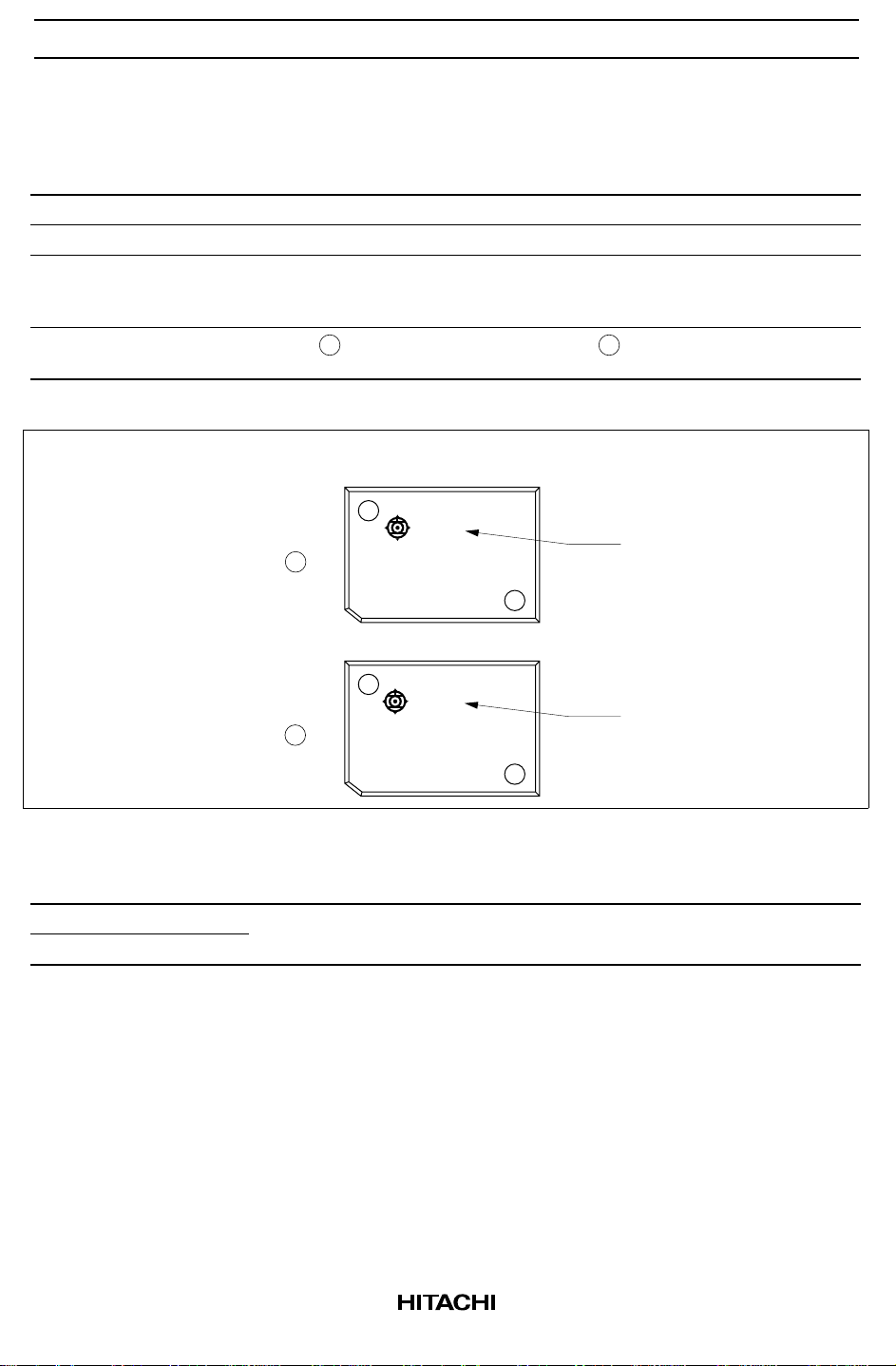
Package marking
to see figure
Pin 6: C
Pin 7: R
Pin 9: CPO
A
Package Marking
Pin 6: CE
Pin 7: OE
Pin 9: NC
B
3D13
A
B
HD61830A00
3D13
HD61830B00
Ordering Information
Type No. Package
HD61830A00H 60-pin plastic QFP (FP-60)
HD61830B00H
Lot No.
JAPAN
Lot No.
JAPAN
3
HD61830/HD61830B
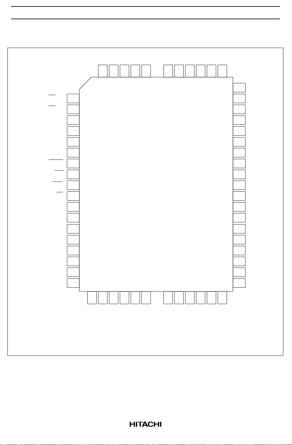
Pin Arrangement
MB
5
MA0
4
MA1
3
MA2
2
MA3
1
MA4
60
MA5
59
MA6
58
MA7
57
MA8
56
MA9
55
54
MA10
(CE) C
(OE) R
CR
(NC) CPO
FLM
CL1
SYNC
WE
RES
CS
R/W
RS
MA
GND
DB7
DB6
6
7
8
9
10
11
12
13
14
15
E
16
17
18
19
20
21
22
FP-60
(Top view)
53
52
51
50
49
48
47
46
45
44
43
42
41
40
39
38
37
MA11
MA12
MA13
MA14
MA15
D2
D1
CL2
RD0
RD1
RD2
RD3
RD4
RD5
RD6
RD7
MD0
( ) is for HD61830B
4
DB5
23
24
DB4
25
DB3
26
DB2
27
DB1
28
DB0
29
V
CC
30
MD7
31
MD6
32
MD5
33
MD4
34
MD3
36
35
MD2
MD1

HD61830/HD61830B
Terminal Functions
Symbol Pin Number I/O Function
DB0–DB7 28–21 I/O Data bus: Three-state I/O common terminal
CS 15 I Chip select: Selected state with CS = 0
R/W 17 I Read/Write:R/W = 1: MPU ← HD61830
RS 18 I Register select:RS = 1: Instruction register
E 16 I Enable: Data is written at the fall of E
CR 8 I CR oscillator (HD61830), External clock input (HD61830B)
C 6 — CR oscillator to capacitor (HD61830 only)
R 7 — CR oscillator to resistor (HD61830 only)
CPO 9 O Clock signal for HD61830 in slave mode (HD61830 only)
CE 6 O Chip enable (HD61830B only)
OE 7 O Output enable (HD61830B only)
NC 9 Open Unused terminal. Don’t connect any wires to this terminal
MA0–MA15 4–1, 60–49 O External RAM address output
MD0–MD7 37–30 I/O Display data bus: Three-state I/O common terminal
RD0–RD7 45–38 I ROM data input: Dot data from external character generator is input
WE 13 O Write enable: Write signal for external RAM
CL2 46 O Display data shift clock for LCD drivers
CL1 11 O Display data latch signal for LCD drivers
FLM 10 O Frame signal for display synchronization
MA 19 O Signal for converting liquid crystal driving signal into AC, A type
MB 5 O Signal for converting liquid crystal driving signal into AC, B type
D1 47 O Display data serial output
D2 48
Data is transferred to MPU through DB0 to DB7.
R/W = 0: MPU → HD61830
RS = 0: Data register
Data can be read while E is 1
CE = 0: Chip enables make external RAM in active
OE = 1: Output enable informs external RAM that HD61830B requires
data bus
(HD61830B only)
In character mode, the line code for external CG is output through
MA12 to MA15 (0: Character 1st line, F: Character 16th line)
D1: For upper half of screen
D2: For lower half of screen
SYNC 12 I/O Synchronous signal for parallel operation
Three-state I/O common terminal (with pull-up MOS)
Master: Synchronous signal is output
Slave: Synchronous signal is input
RES 14 I Reset: Reset = 0 results in display off, slave mode and Hp = 6
5
HD61830/HD61830B
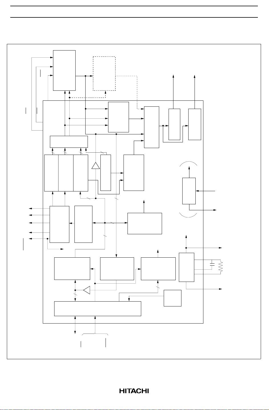
Block Diagram
(CE)
CL1 MAMB FLM
WE
(OE)
16
16
(RAC1)
counter (1)
Refesh address
Dot counter
RAM
counter (2)
Refesh address
(DC)
MD0–MD7
*
Multiplexer
16
(CAC)
(RAC2)
counter
Cursor address
8
(DR)
Dot registers
ROM
external
Extended
Character
4
counter
Line address
8
6
8
ROM
generator
(CGROM)
Cursor
RD0–RD7
signal
generator
Mode
control
Multiplexer
Control
signal
(MCR)
register
D1
converter
Parallel/serial
D2
Parallel/serial
circuit
Oscillator
converter
are applied to RAM, MA12 –MA15 are applied to
extended external ROM.
* When extended external ROM is used, MA0–MA11
(CR)
(CL2)
( ) is for HD61830B
SYNC
Data
input
8
(DIR)
register
CSERS
DB0–DB7
Data
output
register
I/O interface circuit
R/W
RES
(DOR)
Control
signal
(IR)
register
Instruction
4
Busy
flag
Oscillator
(BF)
circuit
CPOR
f
C
f
CL2
6

HD61830/HD61830B
Block Functions
Registers
The HD61830/HD61830B has the five types of registers: instruction register (IR), data input register (DIR),
data output register (DOR), dot registers (DR), and mode control register (MCR).
The IR is a 4-bit register that stores the instruction codes for specifying MCR, DR, a start address register,
a cursor address register, and so on. The lower order 4 bits DB0 to DB3 of data buses are written in it.
The DIR is an 8-bit register used to temporarily store the data written into the external RAM, DR, MCR,
and so on.
The DOR is an 8-bit register used to temporarily store the data read from the external RAM. Cursor address
information is written into the cursor address counter (CAC) through the DIR. When the memory read
instruction is set in the IR (latched at the falling edge of E signal), the data of external RAM is read to DOR
by an internal operation. The data is transferred to the MPU by reading the DOR with the next instruction
(the contents of DOR are output to the data bus when E is at the high level).
The DR are registers used to store dot information such as character pitches and the number of vertical
dots, and so on. The information sent from the MPU is written into the DR via the DIR.
The MCR is a 6-bit register used to store the data which specifies states of display such as display on/off
and cursor on/off/blink. The information sent from the MPU is written in it via the DIR.
Busy Flag (BF)
The busy flag = 1 indicates the HD61830 is performing an internal operation. Instructions cannot be
accepted. As shown in Control Instruction, read busy flag, the busy flag is output on DB7 under the
conditions of RS = 1, R/W = 1, and E = 1. Make sure the busy flag is 0 before writing the next instruction.
Dot Counters (DC)
The dot counters are counters that generate liquid crystal display timing according to the contents of DR.
7

HD61830/HD61830B
Refresh Address Counters (RAC1/RAC2)
The refresh address counters, RAC1 and RAC2, control the addresses of external RAM, character generator
ROM (CGROM), and extended external ROM. The RAC1 is used for the upper half of the screen and the
RAC2 for the lower half. In the graphic mode, 16-bit data is output and used as the address signal of
external RAM. In the character mode, the high order 4 bits (MA12–MA15) are ignored. The 4 bits of line
address counter are output instead and used as the address of extended ROM.
Character Generator ROM
The character generator ROM has 7360 bits in total and stores 192 types of character data. A character code
(8 bits) from the external RAM and a line code (4 bits) from the line address counter are applied to its
address signals, and it outputs 5-bit dot data.
The character font is 5 × 7 (160 characters) or 5 × 11 (32 characters). The use of extended ROM allows 8 ×
16 (256 characters max.) to be used.
Cursor Address Counter
The cursor address counter is a 16-bit counter that can be preset by instruction. It holds an address when the
data of external RAM is read or written (when display dot data or a character code is read or written). The
value of the cursor address counter is automatically increased by 1 after the display data is read or written
and after the set/clear bit instruction is executed.
Cursor Signal Generator
The cursor can be displayed by instruction in character mode. The cursor is automatically generated on the
display specified by the cursor address and cursor position.
Parallel/Serial Conversion
The parallel data sent from the external RAM, character generator ROM, or extended ROM is converted
into serial data by two parallel/serial conversion circuits and transferred to the liquid crystal driver circuits
for upper screen and lower screen simultaneously.
8
HD61830/HD61830B
y
Display Control Instructions
Display is controlled by writing data into the instruction register and 13 data registers. The RS signal
distinguishes the instruction register from the data registers. 8-bit data is written into the instruction register
with RS = 1, and the data register code is specified. After that, the 8-bit data is written in the data register
and the specified instruction is executed with RS = 0.
During the execution of the instruction, no new instruction can be accepted. Since the busy flag is set
during this, read the busy flag and make sure it is 0 before writing the next instruction.
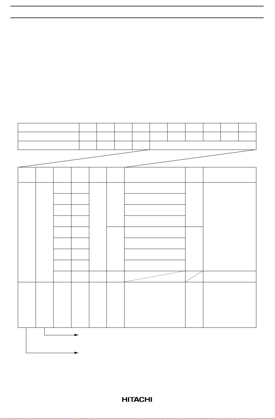
1. Mode Control: (Execution time: 4 µs) Code H'00 (hexadecimal) written into the instruction register
specifies the mode control register.
Register
Instruction reg.
Mode control reg.
DB5 DB4 DB3 DB2 DB1 DB0 Cursor/blink CG
1/0 1/0 0
0
1
1
0
0
1
1
0
0
1
0
1
0
1
0
1
0
R/W
0
0
RS
DB7
1
0
0
1
0
1
0
DB6
0
0
Cursor off
Cursor on
Cursor off, character blink
Cursor blink
Cursor off
Cursor on
Cursor off, character blink
Cursor blink
DB50DB40DB30DB20DB10DB0
0
0
Mode data
0
Graphic/character
display
Character display
(Character mode)
Internal CGExternal CG
Graphic mode
Display ON/OFF
Master/slave
Blink
Cursor
Graphic/character
mode
1: Master mode
0: Slave mode
1: Display ON
0: Displa
OFF
Ext./Int. CG
9

HD61830/HD61830B
2. Set Character Pitch: (Execution time: 4 µs) Vp indicates the number of vertical dots per character. The
space between the vertically-displayed characters is included in the determination. This value is meaningful
only during character display (in the character mode) and becomes invalid in the graphic mode.
Hp indicates the number of horizontal dots per character in display, including the space between
horizontally-displayed characters. In the graphic mode, the Hp indicates the number of bits of 1-byte display
data to be displayed.
There are three Hp values (Table 1).
Register R/W RS DB7 DB6 DB5 DB4 DB3 DB2 DB1 DB0
Instruction reg. 0 1 0 0 0 0 0 0 0 1
Character pitch reg. 0 0 (Vp – 1) binary 0 (Hp – 1) binary
Table 1 Hp Values
H
p
61016
71107
81118
DB2 DB1 DB0 Horizontal Character Pitch
10
HD61830/HD61830B
3. Set Number of Characters: (Execution time: 4 µs) HN indicates the number of horizontal characters in
the character mode or the number of horizontal bytes in the graphic mode. If the total sum of horizontal
dots on the screen is taken as n,
n = Hp × H
N
HN can be set to an even number from 2 to 128 (decimal).
Register R/W RS DB7 DB6 DB5 DB4 DB3 DB2 DB1 DB0
Instruction reg. 0 1 0 0 0 0 0 0 1 0
Number-of-characters reg. 0 0 0 (HN – 1) binary
4. Set Number of Time Divisions (Inverse of Display Duty Ratio): (Execution time: 4 µs) NX indicates
the number of time divisions in multiplex display.
1/NX is the display duty ratio.
A value of 1 to 128 (decimal) can be set to NX.
Register R/W RS DB7 DB6 DB5 DB4 DB3 DB2 DB1 DB0
Instruction reg. 0 1 0 0 0 0 0 0 1 1
Number-of-time-divisions reg. 0 0 0 (NX – 1) binary
5. Set Cursor Position: (Execution time: 4 µs) Cp indicates the position in a character where the cursor is
displayed in the character mode. For example, in 5 × 7 dot font, the cursor is displayed under a character by
specifying Cp = 8 (decimal). The cursor horizontal length is equal to the horizontal character pitch Hp. A
value of 1 to 16 (decimal) can be set to Cp. If a smaller value than the vertical character pitch Vp is set (C
≤ Vp), and a character overlaps with the cursor, the cursor has higher priority of display (at cursor display
on). If Cp is greater than Vp, no cursor is displayed. The cursor horizontal length is equal to Hp.
p
Register R/W RS DB7 DB6 DB5 DB4 DB3 DB2 DB1 DB0
Instruction reg. 0 1 0 0 0 0 0 1 0 0
Cursor position reg. 0 0 0 0 0 0 (Cp – 1) binary
11

HD61830/HD61830B
6. Set Display Start Low Order Address: (Execution time: 4 µs) Cause display start addresses to be
written in the display start address registers. The display start address indicates a RAM address at which the
data displayed at the top left end on the screen is stored. In the graphic mode, the start address is composed
of high/low order 16 bits. In the character display, it is composed of the lower 4 bits of high order address
(DB3–DB0) and 8 bits of low order address. The upper 4 bits of high order address are ignored.
Register R/W RS DB7 DB6 DB5 DB4 DB3 DB2 DB1 DB0
Instruction reg. 0 1 0 0 0 0 1 0 0 0
Display start address reg.
(low order byte)
Set Display Start High Order Address
Register R/W RS DB7 DB6 DB5 DB4 DB3 DB2 DB1 DB0
Instruction reg. 0 1 0 0 0 0 1 0 0 1
Display start address reg.
(high order byte)
0 0 (Start low order address) binary
0 0 (Start high order address) binary
7. Set Cursor Address (Low Order) (RAM Write Low Order Address): (Execution time: 4 µs) Cause
cursor addresses to be written in the cursor address counters. The cursor address indicates an address for
sending or receiving display data and character codes to or from the RAM.
That is, data at the address specified by the cursor address are read/written. In the character mode, the
cursor is displayed at the character specified by the cursor address.
A cursor address consists of the low-order address (8 bits) and the high-order address (8 bits). Satisfy the
following requirements setting the cursor address (Table 2).
The cursor address counter is a 16-bit up-counter with set and reset functions. When bit N changes from 1
to 0, bit N + 1 is incremented by 1. When setting the low order address, the LSB (bit 1) of the high order
address is incremented by 1 if the MSB (bit 8) of the low order address changes from 1 to 0. Therefore, set
both the low order address and the high order address as shown in the Table 2.
Register R/W RS DB7 DB6 DB5 DB4 DB3 DB2 DB1 DB0
Instruction reg. 0 1 0 0 0 0 1 0 1 0
Cursor address counter
(low order byte)
0 0 (Cursor low order address) binary
12

HD61830/HD61830B
Set Cursor Address (High Order) (RAM Write High Order Address)
Register R/W RS DB7 DB6 DB5 DB4 DB3 DB2 DB1 DB0
Instruction reg. 0 1 0 0 0 0 1 0 1 1
Cursor address counter
(high order byte)
Table 2 Cursor Address Setting
Condition Requirement
When you want to rewrite (set ) both the low order
address and the high order address.
When you want to rewrite only the low order address. Do not fail to set the high order address again after
When you want to rewrite only the high order address. Set the high order address. You do not have to set
0 0 (Cursor high order address) binary
Set the low order address and then set the high
order address.
setting the low order address.
the low order address again.
13
 Loading...