

HIT HD49323AF-01 Datasheet
HD49323AF-01
CDS/AGC & 10-bit A/D Converter
ADE-207-262A (Z)
2nd Edition
Apr. 1999
Description
The HD49323AF-01 is a CMOS IC that provides CCD-AGC analog processing (CDS/AGC) suitable for
CCD camera digital signal processing systems together with a 10-bit A/D converter in a single chip.
Functions
• Correlated Double Sampling
• AGC
• Sample hold
• Offset compensation
• Serial interface control
• 10-bit ADC
• 3 V single operation (2.7 V to 3.6 V)
• Power dissipation: 198 mW (Typ)
• Maximum frequency: 20 MHz (Min)
Features
• Good suppression of CCD output low-frequency noise is achieved through the use of S/H type
correlated double sampling.
• A high S/N ratio is achieved through the use of a AGC type amplifier, and high sensitivity is provided
by a wide cover range.
• An auto offset circuit provides compensation of output DC offset voltage fluctuations due to variations
in AGC amplifier gain.
• AGC, standby mode, offset control, etc., is possible via a serial interface.
• High precision is provided by a 10-bit-resolution A/D converter.
• Version of Hitachi’s previous-generation HD49322BF with improved functions and performance,
including in particular an approximately 3.0 dB improvement in S/N.
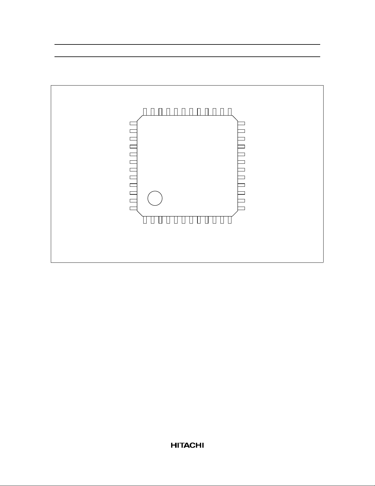
HD49323AF-01
Pin Arrangement
NC
BIAS
VRT
VRM
VRB
AVDDAVSSTESTC
TESTY
CDSIN
AVDDAV
SS
AV
SS
AV
DD
NC
NC
AV
DD
AV
SS
CS
SCK
SDATA
DV
DD
DV
SS
DV
SS
36 35 2734 33 32 31 30 29 28 26 25
37
38
39
40
41
42
43
44
45
46
47
48
12 103456789 1112
D0D1D2D3D4D5D6D7D8
PBLK
(Top view)
D9
24
23
22
21
20
19
18
17
16
15
14
13
NC
VRM2
CLP
NC
AV
DD
AV
SS
SPSIG
SPBLK
OBP
ADCLK
DV
DD
DV
SS
OE
2

HD49323AF-01
Pin Description
Analog(A) or
Pin No. Symbol Description I/O
1 PBLK Pre-blanking pin I D
2 D0 Digital output (LSB) O D
3 to 10 D1 to D8 Digital output O D
11 D9 Digital output (MSB) O D
12 NC No connection pin — —
13 OE Digital output enable control pin I D
14 DV
15 DV
SS
DD
Digital ground (0 V) — D
Digital power supply (3 V)
Connect off-chip in common with AV
.
DD
16 ADCLK ADC conversion clock input pin I D
17 OBP Optical black pulse input pin I D
18 SPBLK Black level sampling clock input pin I D
19 SPSIG Signal level sampling clock input pin I D
20 AV
21 AV
SS
DD
Analog ground (0 V) — A
Analog power supply (3 V)
Connect off-chip in common with DV
.
DD
22 NC No connection pin — —
23 CLP Clamp voltage pin
Connect a 0.22 µF or more capacitor between CLP and AV
.
SS
24 VRM2 Reference voltage pin (for CCD offset cancel) — A
25 AV
26 AV
SS
DD
Analog ground (0 V) — A
Analog power supply (3 V)
Connect off-chip in common with DV
.
DD
27 CDSIN CDS input pin I A
28 TESTY Test input pin-Y I A
29 TESTC Test input pin-C I A
30 AV
31 AV
SS
DD
Analog ground (0 V) — A
Analog power supply (3 V)
Connect off-chip in common with DV
.
DD
32 VRB Reference voltage pin 3
Connect a 0.1 µF ceramic capacitor between VRB and AV
.
SS
33 VRM Reference voltage pin 2
Connect a 0.1 µF ceramic capacitor between VRM and AV
.
SS
34 VRT Reference voltage pin 1
Connect a 0.1 µF ceramic capacitor between VRT and AV
.
SS
Digital(D)
—D
—A
—A
—A
—A
—A
—A
—A
3
HD49323AF-01
Pin Description (cont)
Analog(A) or
Pin No. Symbol Description I/O
35 BIAS Internal bias pin
Connect a 24 kΩ resistor between BIAS and AVSS.
36 NC No connection pin — —
37 AV
38 AV
SS
DD
Analog ground (0 V) — A
Analog power supply (3 V)
Connect off-chip in common with DV
.
DD
39, 40 NC No connection pin — —
41 AV
42 AV
DD
SS
Analog power supply (3 V)
Connect off-chip in common with DV
.
DD
Analog ground (0 V) — A
43 CS Serial interface control input pin I D
44 SCK Serial clock input pin I D
45 SDATA Serial data input pin I D
46 DV
47, 48 DV
DD
SS
Digital power supply (3 V)
Connect off-chip in common with AV
.
DD
Digital ground (0 V) — D
Digital(D)
—A
—A
—A
—D
4
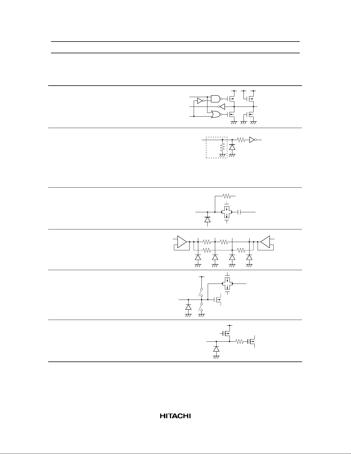
Input/Output Equivalent Circuit
Pin Name Equivalent Circuit
Digital output D0 to D9
DIN
STBY
or
OE
HD49323AF-01
DV
DD
Digital
output
Digital input ADCLK
OBP
SPBLK
SPSIG
CS
SCK
SDATA
PBLK
OE
Analog input CDSIN
Reference voltage input VRT
VRM
VRB
VRM2
Clamp CLP
Digital
input
CDSIN
VRT VRM VRM2
+
−
AV
DD
*1
70kΩ
(Typ)
Connected to
VRM internally
VRB
Connected to
VRM internally
+
−
Internal bias BIAS
Note: 1. Applies to OE and PBLK.
CLP
BIAS
AV
DD
5
HD49323AF-01
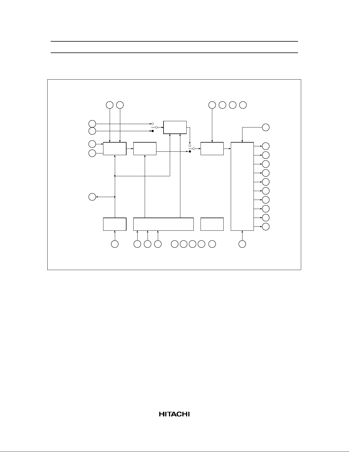
Block Diagram
SPSIG
SPBLK
ADCLK
VRT
VRM
323334161918
VRB
TESTC
TESTY
CDSIN
VRM2
CLP
27
27
27
27
23
Gain
select
CDS AGC
Clamp
circuit
17 44 45 43 35
OBP
Serial interface
SCK
CS
SDATA
DD
AV
DD
DV
SS
AV
10bit
ADC
Bias
ganerator
SS
BIAS
DV
OE11
D9
11
D8
10
D7
9
D6
8
D5
7
D4
6
D3
5
Output latch circuit
17
PBLK
D2
4
D1
3
D0
2
6
HD49323AF-01
Internal Functions
Functional Description
• CDS (Correlated Double Sampling) circuit
• AGC gain selection (11-bit digital control) *
AGC gain can be set in the range 0 dB to 34.7 dB on the (+) side, and –3.3 dB to 0 dB on the (–)
side by means of 11-bit serial data.
• Automatic offset adjustment is possible for the IC’s offsets (CDS, AGC, ADC) by means of serial data
control at power-on.*
1
• Digital output enable function
• Pre-blanking function
Digital output can be fixed at 32 LSB
• CDS offset cancel function
Note: 1. Serial data control
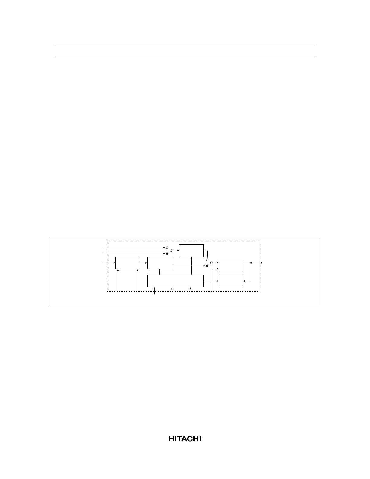
Operating Description
Figure 1 shows CDS/AGC +ADC function block.
1
TESTC
TESTY
CDSIN
CDS
SPBLK ADCLK
SPSIG SDATA
AGC
Serial interface
CS SCK
Gain
select
10bit
ADC
Offset
cancel
D0 to D9
Figure 1 CDS/AGC +ADC Function Block
1. CDS (Correlated Double Sampling) Circuit
The CCD imaging element alternately outputs a black level (A-period signal) and a signal including the
black level (B-period signal). The CDS circuit extracts the differential voltage between the black level
and the signal including the black level (see figure 4).
Black level sampling is performed at the rising edge of the SPBLK pulse, and signal level sampling is
performed at the rising edge of the SPSIG pulse. This sequence of operations extracts the differential
voltage between the black level and the signal including the black level, and supplies this to the nextstage AGC circuit.
2. Feed back clamp function
The clamp level is set by means of 5-bit serial data. The setting range is 32 LSB to 56 LSB, in 1 LSB
steps. A serial data value of 0 gives a 32 LSB setting, and a value of 24 gives a 56 LSB setting.
7
HD49323AF-01
3. AGC Circuit
The AGC gain is set by means of 11-bit serial data. The setting range is –3.3 dB to 34.7 dB. Details of
the data are given in the following section.
The (–) side gain setting uses setting codes –81 to 0 in 0.0039-multiple steps, and the (+) side gain
setting uses setting codes 0 to 1023 in 0.034 dB steps.
• Detailed specifications of HD49323AF-01 AGC gain setting codes
(1) To improve S/N, the AD input dynamic range has been extended to 1.4 V from the 1.0 V of the
HD49322BF.
(2) There are two AGC gain ranges: (+) side 0 to 34.7 dB linear gain amp. (0.034 dB/step), and (–) side
0 to –3.3 dB “multiple” linear gain amp. (0.0039 multiple/step).
Range
CDS AGC ADC
Typ 1.4V
0V = 0 code
0.7V = 511 code
1.4V = 1023 code
OutputInput
Considering the case where AGC gain is set so that the ADC output code is 511 when a 150 mV signal is
input:
The HD49322BF AGC gain setting is (code 511)/150 mV multiple = 500 mV/150 mV multiple
The HD49323AF-01 AGC gain setting is (code 511)/150 mV multiple = 700 mV/150 mV multiple
Table 2 AGC Gain (−) Setting Code TableTable 1 AGC Gain (+) Setting Code Table
Code BIN (D10 to D0) dB
0 000 0000 0000 0.000
1 000 0000 0001 0.034
2 000 0000 0010 0.068
3 000 0000 0011 0.102
⋅
⋅
⋅
510 001 1111 1110 17.34
511 001 1111 1111 17.37
512 010 0000 0000 17.41
513 010 0000 0001 17.44
⋅
⋅
⋅
1020 011 1111 1100 34.68
1021 011 1111 1101 34.71
1022 011 1111 1110 34.75
1023 011 1111 1111 34.78
Code BIN (D10 to D0) Multiple
0 000 0000 0000 1.000
−1 111
−2 1111 1110 0.992
−3 111 1111 1101 0.988
⋅
⋅
⋅
−30 111 1110 0010 0.883
−31 111 1110 0001 0.879
−32 111 1110 0000 0.875
−33 111 1101 1111 0.871
⋅
⋅
⋅
−78 111 1011 0010 0.695
−79 111 1011 0001 0.691
−80 111 1011 0000 0.688
−81 111 1010 1111 0.684
1111 1111 0.996
111
dB
0.000
−0.034
−0.068
−0.102
−1.083
−1.121
−1.160
−1.199
−3.156
−3.205
−3.255
−3.304
4. Offset cancel circuit
When power is turned on, offset voltages generated by CDS, AGC, ADC, and other circuits by means
of serial data control are canceled. (Refer to page 24 (Operating Sequence at Power-On).)
8
HD49323AF-01
5. Digital output enable function
When the OE pin is driven high, digital output goes to the high-Z state.
OE Pin Digital Output
High High-Z state
Low (or Open, GND) Output enable
6. Pre-blanking function
When the PBLK pin is driven high, digital output is fixed at 32 LSB. However, this is valid only when
the OE pin and serial data output mode settings (LINV, MINV, TEST, STBY) are low.
PBLK Pin Digital Output
High Fixed at 32 LSB
Low (or Open, GND) Active
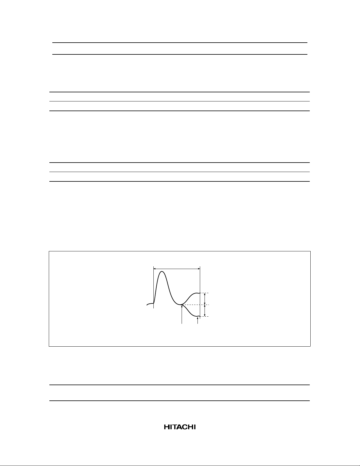
7. CCD offset cancel function
This function cancels the offset voltage (V
element. The definition of the CCD offset voltage (V
) during the optical black period of the CCD imaging
OFCCD
) is given below.
OFCCD
• The difference between the black level sampling voltage and signal level sampling voltage during the
OBP period is designated V
. This value is positive when (signal level sampling voltage) > (black
OFCCD
level sampling voltage).
Input signal for one pixel
(during OBP period)
CDS input
Black level
sampling
point
V
OFCCD
V
OFCCD
Signal level
sampling
point
(at +)
(at −)
Figure 2 Black Level Signal Level Difference during OBP Period
Table 3 Serial Data Settings
V
Cancel Function When Used When Not Used
OFCCD
Serial data settings VOFCON bit set to 1
VOFD0—3 (4 bits) set
VOFCON bit cleared to 0
9
 Loading...