

HIT HD49235FS Datasheet

HD49235FS
Digital Signal Processor for CD
ADE-207-162A(Z)
2nd. Edition
August 1995
Description
The HD49235FS is a digital signal processor for compact disc (CD) applications.
Features
• Powerful error correction capability: two-symbol C1 correction and four-symbol C2 correction
• Quadruple-speed reproduction supported (maintaining two-symbol C1 and four-symbol C2 error
correction)
• On-chip analog PLL and digital PLL (VCO and phase detector)
• Automatic adjustment of the free-running frequency of the VCO
• Built-in microprocessor in terface
• On-chip 80-bit shift registers for Q-code buffering
• Cyclic redundancy check on Q-code values
• Audio output functions: monaural output, single-channel mute, left-right reverse, soft mute, –12-dB
attenuation
• 16-kbit RAM on-chip
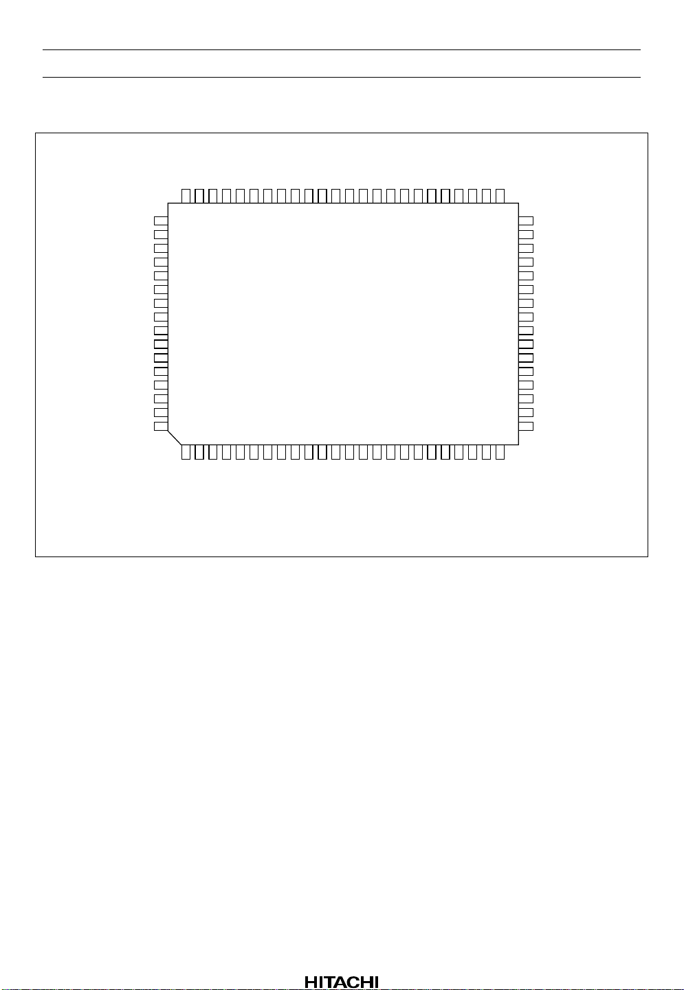
HD49235FS
Pin Arrangement
QDSEL
DSLCO
DSLCI
EFMI
DEFCT
TEST2
TEST3
UCKSL
V (D)
DD
PWM
MON
MSTOP
PW64
ROTD
CLVS
SLOCK
DD
PDOUT1
V (A)
AMPP
AMPM
SS
AMPOACV (A)
PDOUT2
TEST1
MRST
DD
PLLCKNCV (D)NCNCNCNCNCNCNCNCNCNC
64 41
65
80
CNIN
XRST
DATA
SENS
CLK
XLT
SS
OVFW
V (D)
QOK
CKEXT
QDATA
CFCKP
SUBCK
SUBOUT
EMP
MUTE
BIDAT
DAS
CKX
MPX
C2F
S1
(Top view)
241
QMX
NC
40
25
DMX
NC
NC
NC
NC
NC
NC
NC
NC
NC
V (D)
SS
XCI
XCO
NC
MCK
TC1
UCK
Rev.2, Aug. 1995, page 2 of 41
HD49235FS
Pin Description
Pin Polarity
No. Symbol Name I/O* Connection Function H L
1 XRST X (µ-com)
reset
2 CNIN Counter clock
input
3 SENS Sensor TO Microprocessor Servo status output
4 DATA Data I Microprocessor Data input for microprocessor
5 CLK Clock I Microprocessor Clock input for microprocessor
6 XLT X (µ-com) latch I Microprocessor Strobe input for
7VSS (D) VSS (digital) — Digital ground
8 OVFW RAM- overflow O On-chip RAM overflow signal
9 S1 Subcode sync1O Microprocessor Subcode sync signal
10 QOK Q-code OK O Microprocessor Subcode CRC result output OK NG
11 QDATA Q-code data O Microprocessor Subcode Q data output
12 CKEXT Clock-EXT I Microprocessor Clock input for Q data readout
13 SUBOUT Subcode out O CD graphics Subcode data output for CD
14 SUBCK Subcode clock I CD graphics Clock input for SUBOUT
15 CFCKP C&D frame
clock out
16 EMP Emphasis
output
17 BIDAT Biphase date TO Digital audio interface output
18 MUTE Mute I Microprocessor Audio mute input Mute
19 DAS Data serial out O DAC or ROM
20 CKX Clock X O DAC or ROM
I Microp rocessor Microprocessor interface
register reset
I Servo IC Pulse input for track counter
interface
interface
microprocessor interface
output
(with protection)
graphics
subcode readout
O CD graphics Subcode frame
synchronization signal ( 7.35
kHz at normal speed,
synchronized with PLL)
O Emphasis on/off status output ON OFF
Serial data output for audio or
decoder
decoder
ROM
Strobe clock output for DAS
signal
Reset
Overflow
Rev.2, Aug. 1995, page 3 of 41
HD49235FS
Pin Description (cont)
Pin Polarity
No. Symbol Name I/O* Connection Function H L
21 MPX Multiplex O DAC or ROM
decoder
22 C2F C2 flag O ROM decoder C2 error flag output Error
23 QMX Quad multiplex O 4 × MPX clock signal
24 DMX Double
multiplex
25 UCK µ-com clock O Microprocessor Clock output for
26 TC1 Test C1 flag O C1 error flag monitor pin Error
27 MCK Master clock O Master clock output
28 NC No connection — Open or VDD Not connected
29 XCO X’tal clock
output
30 XCI X’tal clock
input
31 VSS (D) VSS (digital) — Digital ground
32 NC No connection — Open Not connected
33 NC No connection — Open Not connected
34 NC No connection — Open Not connected
35 NC No connection — Open Not connected
36 NC No connection — Open Not connected
37 NC No connection — Open Not connected
38 NC No connection — Open Not connected
39 NC No connection — Open Not connected
40 NC No connection — Open Not connected
41 NC No connection — Open Not connected
42 NC No connection — Open Not connected
43 NC No connection — Open Not connected
44 NC No connection — Open Not connected
O2 × MPX clock signal
XO Crystal
oscillator
XI Crystal
oscillator
Left/right channel switching
signal output (44.1 kHz at
normal speed, synchronized
with DAS)
(176.4 kHz at normal speed,
synchronized with DAS)
(88.2 kHz at normal speed,
synchronized with DAS)
microprocessor
(8.5 MHz or 17 MHz)
(33.8688 MHz)
Crystal oscillator output
Crystal oscillator input
Rev.2, Aug. 1995, page 4 of 41
HD49235FS
Pin Description (cont)
Pin Polarity
No. Symbol Name I/O* Connection Function H L
45 NC No connection — Open Not connected
46 NC No connection — Open Not connected
47 NC No connection — Open Not connected
48 NC No connection — Open Not connected
49 NC No connection — Open Not connected
50 NC No connection — Open Not connected
51 NC No connection — Open Not connected
52 VDD (D) VDD (digital) — Digital power supply
53 NC No connection — Open or V
54 PLLCK PLL clock O PLL clock output monitor
55 MRST Master reset IU Open or V
56 TEST1 TEST 1 IU Open or V
57 PDOUT2 Phase detect
out 2
TO External RC
circuit
58 VSS (A) VSS (analog) — Analog ground
59 AC Amp
compensation
AExternal RC
circuit
60 AMPO Amp output AO External RC
circuit
61 AMPM Amp minus
input
AI External RC
circuit
62 AMPP Amp plus input AI External RC
circuit
63 VDD (A) VDD (analog) — Analog power supply
64 PDOUT1 Phase detect
out 1
65 QDSEL Q-data clock
TO External RC
circuit
IU Q data readout mode
select
66 DSLCO DSL control
output
67 DSLCI DSL control
input
68 EFMI EFM signal
OExternal RC
circuit
AI External RC
circuit
AI EFM signal input
input
69 DEFCT Defect I Servo IC Defect detection signal input Defect
70 TEST2 TEST 2 IU Open or V
Not connected
DD
Master reset of chip Reset
DD
Test pin
DD
PLL auto-adjust phase
detector output
Amplifier phase compensat ion
pin
PLL amplifier output
PLL amplifier inverting input
PLL amplifier non-inverting
input
PLL EFM phase detector
output
Internal
switching signal input
sync
EFM comparator slice level
control output
EFM comparator slice level
control input
Test pin
DD
External
sync
Rev.2, Aug. 1995, page 5 of 41
HD49235FS
Pin Description (cont)
Pin Polarity
No. Symbol Name I/O* Connection Function H L
71 TEST3 TEST 3 IU Open or V
72 UCKSL Microcomputer
clock selection
73 VDD (D) VDD (digital) — Digital power supply
74 PWM Pulse width
modulate
75 MON Motor on O Disc-motor-on status detection
76 MSTOP Motor stop TO CLV phase control signal
77 PW64 Pulse width
64T
78 ROTD Rotate
direction
79 CLVS CLV status O Microprocessor Output indicating normal or
80 SLOCK Sync lock O Microprocessor Disc motor rotation lock signal Lock
Note: * I—input; O—output; IO—input/output; IU—pulled-up input; TO—three-state output; A—analog pin;
AI—analog input; AO—analog output; XI—oscillator input; XO—oscillator output
IU Microprocessor clock
TO Constant linear velocity (CLV)
O Microprocessor Brake release signal
O Microprocessor MSB of PWM pin output, for
Test pin
DD
switching signal input
control signal for disc motor
output
monitoring
starting mode of CLV control
16.9344
MHz
On
Normal Starting
8.4672
MHz
Rev.2, Aug. 1995, page 6 of 41
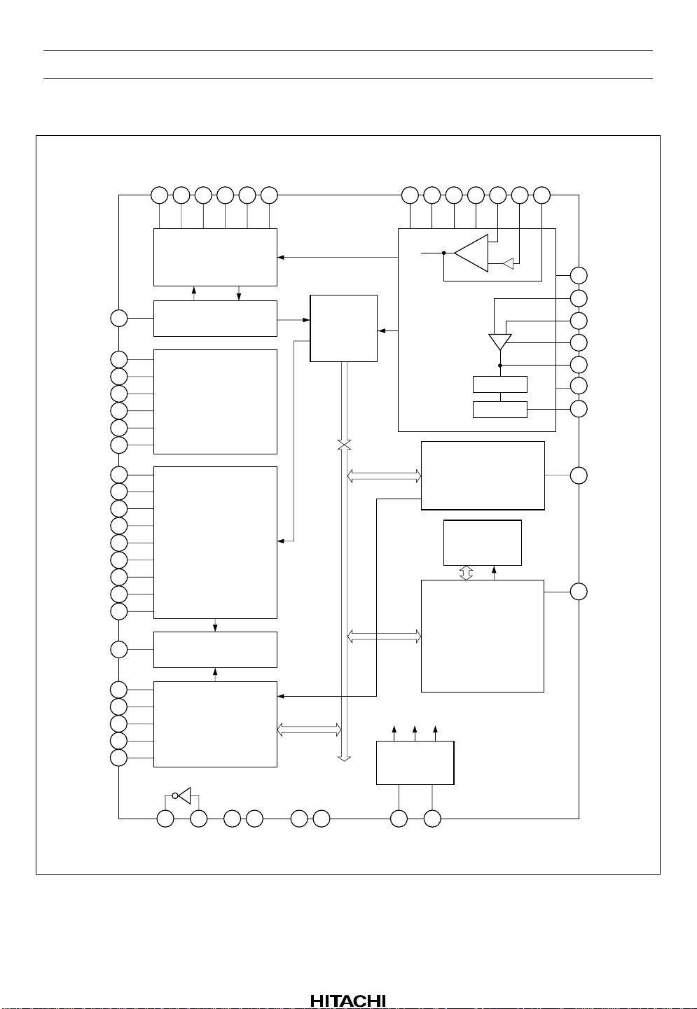
Block Diagram
CLVS
ROTD
PW64
MSTOP
MON
PWM
79 78 77 76 75 74 72 25 27 69 68
UCKSL
UCK
MCK
DEFCT
EFMI
67
HD49235FS
DSLCI
DSLCO
66
SLOCK
XRST
CNIN
SENS
DATA
CLK
XLT
QDSEL
S1
QOK
QDATA
CKEXT
SUBOUT
SUBCK
CFCKP
EMP
BIDAT
80
65
10
11
12
13
14
15
16
17
CLV servo control
Sync protection
1
2
3
4
5
6
9
Microprocessor
interface
Subcode signal
processing
Digital output
demodula-
Data bus
EFM
Data strobe
tion
Cmp
+
-
VCO
Freq. Div.
Error correction unit
(ECU)
16 k SRAM
RAM control
64
62
61
59
60
57
54
26
8
PDOUT1
AMPP
AMPM
AC
AMPO
PDOUT2
PLLCK
TC1
OVFW
MUTE
DAS
CKX
MPX
C2F
18
19
20
21
22
Interpolation
XCI
XCO
MRST
TEST1
TEST2
TEST3
Timing
generator
2423717056553029
QMX
DMX
Rev.2, Aug. 1995, page 7 of 41
HD49235FS
Microprocessor Commands
Data
SENS
Register
(Address) Command D7 D6 D5 D4 D3 D2 D1 D0
8 (1000) Mode
selections
9 (1001) Function
selections
A (1010) Audio
control
B (1011) Trac k
counter
setting
C (1100) CLV control AINTV ATH GA IN1 GAIN0 SGAIN1 SGAIN0 PDGAIN1 PDGAIN0 Count
D (1101) CLV kick
control
E (1110) CLV m ode ED3 ED2 ED1 ED0 0 * * * BRAKE
F (1111) ECU mode 0 0 AS0 * * * * * Z
ROM ROMEF DOOFF SUBCO SLTSW 0 DCOND DWIDTH Z
1 BI1 BI0 WG10TL SYLCK1 SYLCK0 CRCQ * Z
MUTEL MUTER MONO ATT BLGMAIN BLGSUB SOFTMT SWLR Z
TC7 TC6 TC5 TC4 TC3 TC2 TC1 TC0 Complete
KICK7 KICK6 KICK5 KICK4 KICK3 KICK2 KICK1 * Z
Asterisks indicate don’t-care bits
Pin
Output
Register 8
01
ROM D7 Audio (with interpolation) CD-ROM (no interpolation)
ROMEF D6 C2 flag output order: lower first C2 flag output order: upper first
DOOFF D5 Digital output on Digital output off
SUBCO D4 Subcode data not inserted in DAS signal Subcode data inserted in DAS signal
SLTSW D3 48-fs clock 64-fs clock
D2 Normal operation Illegal setting
DCOND D1 Condition for switching between digital and
analog PLLs: digital PLL when defect
detection signal width is 4 frames or more
DWIDTH D0 Digital PLL termination timing:
• 8 frames after fall of defect detection
signal if width of defect detection signal
width is less than 12 frames
• 16 frames after fall of defect detection
signal if width of defect detection signal
width is 12 frames or more
Condition for switching between digital and
analog PLLs: digital PLL when defect
detection signal width is 8 frames or more
• 4 frames after fall of defect detection
signal if width of defect detection signal
width is less than 12 frames
• 8 frames after fall of defect detection
signal if width of defect detection signal
width is 12 frames or more
Rev.2, Aug. 1995, page 8 of 41
HD49235FS
Register 9
01
D7 Illegal setting Normal operation
BI1 D6 00: Normal play 01: Double-speed play
BI0 D5 10: Quadruple-speed play 11: Quadruple-speed play
WG10TL D4 Sync detection window width: ±10 T Sync detection window width: ±19 T
SYLCK1 D3 Length of time sync lock state is maintained when sync signal is missing
SYLCK0 D2 00: 2 frames 01: 4 frames
10: 8 frames 11: 12 frames
CRCQ D1 QOK flag is not inserted in QDATA output QOK flag is inserted in QDATA output
Register A
01
MUTEL D7 Left-channel mute off Left-channel mute on
MUTER D6 Right-channel mute off Right-channel mute on
MONO D5 Stereo Monaural
ATT D4 Attenuation off Attenuation (–12 dB) on
BLGMAIN D3 00: Stereo 01: Bilingual, right channel
BLGSUB D2 10: Bilingual, left channel 11: Bilingual, left channel
SOFTMT D1 Soft mute off Soft mute on
SWLR D0 Normal Left-right reverse
Notes: 1. Priority for mute and attenation as follows.
“Mute” port > SOFTMT > MUTE L, MUTE R > ATT
2. In the case of setting “ROM” = 1 (CD-ROM mode), the data of register “A” is ignored and is
considered all zero.
It is recovered as it were, after setting “ROM” = 0.
3. “BLGMAIN” and “BLG SUB” commands are ignored if “SWLR” = 1, and set stereo.
Register B
D7 D6 D5 D4 D3 D2 D1 D0
Track counter setting TC7 TC6 TC5 TC4 TC3 TC2 TC1 TC0
1286432168421
Rev.2, Aug. 1995, page 9 of 41
HD49235FS
Register C
01
AINTV D7 Sync detection count is tested at 32-frame
intervals
ATH D6 Sync must be detected 4 times or more Sync must be detected 8 times or more
GAIN1 D5 Speed error (PWM pin output) gain in CLV steady state operation
GAIN0 D4 00: –6 dB 01: 0 dB
10: +6 dB 11: 0 dB
SGAIN1 D3 Speed error gain and access
SGAIN0 D2 00: –6 dB 01: 0 dB
10: +6 dB 11: 0 dB
PDGAIN1 D1 CLV phase error (MSTOP pin output) gain
PDGAIN0 D0 00: –6 dB 01: 0 dB
10: +6 dB 11: 0 dB
Register D
Sync detection count is tested at 64-frame
intervals
D7 D6 D5 D4 D3 D2 D1 D0
CLV kick control KICK7 KICK6 KICK5 KICK4 KICK3 KICK2 KICK1 *
(PWM duty cycle) 64/128 32/128 16/128 8/128 4/128 2/128 1/128 *
Asterisks indicate don’t-care bits
Rev.2, Aug. 1995, page 10 of 41
HD49235FS
CLV Mode
ED3 to ED0/HEX Mode Status
0000 0 STOP Motor stop
0110 6 PLAY Starting mode
1000 8 ROT Disc motor driven forward
1001 9 KICK Kick control
1010 A BRAKE Disc motor driven in reverse
1100 C ACS Access mode
1110 E START Forced starting mode
1111 F NORM Forced normal mode
ECU Mode
AS0 Mode Status
0 FULL Error correction: C1—two symbols; C2—four symbols
1 E4IHD C2—four symbol error correction inhibited on track jump
(Register E)
Normal mode
(Register F)
Rev.2, Aug. 1995, page 11 of 41
HD49235FS
Functional Description
Data Strobe
The main functions of this block are described below.
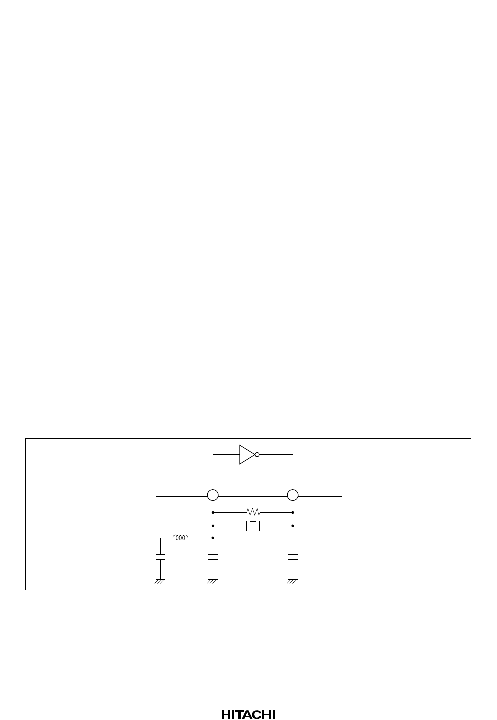
1. Generation of Basic Crystal Clock
Is the inverter input pin for the crystal oscillator.
XCI:
Is the inverter output pin for the crystal oscillator.
XCO:
A 33.8688-MHz crystal oscillator clock signal is generated at the XCI and XCO pins. Figure 1 shows
the standard external components when a 33.8688-MHz crystal is used.
2. Generation of Basic PLL Clock
PLLCK:
the frequency is 4.3218 MHz at standard speed, 8.6436 MHz at double speed, or 17.2872 MHz at
quadruple speed.
PDOUT1:
impedance state in the CLV stop mode. In other CLV modes, this pin outputs the result of phase
detection in a phase-locked loop formed with the VCO and the EFM signal input at the EFMI pin.
PDOUT2:
VCO. In CLV stop mode, this pin outputs a pulse-width modulated waveform equivalent to the phase
error in a phase-locked loop formed with the VCO and a crystal-o scillato r - derived clock signal. In other
CLV modes, this pin maintains a pulse-width modulated output with the same duty cycle as in stop
mode.
AC:
AMPO:
AMPM:
This is an output pin used for monitoring the VCO oscillator sig nal. When the PLL is in lock,
This is a phase detector output pin, for use in data strobing. This pin is in the high-
This is a phase detector output pin, for use in adjusting the free-running frequency of the
Connect a capacitor for phase compensation of the amplifier.
Amplifier output pin.
Inverting input to the amplifier.
Figure 1 33.8688-MHz Crystal Oscillator Circuit
Rev.2, Aug. 1995, page 12 of 41
3.3 µH
100 pF
XCI
30 29
XCO
1 MΩ
15 pF15 pF

HD49235FS
AMPP:
Non-inverting input to the amplifier.
This chip uses a PLL for recovery of the bit clock. A built-in circuit au tomatically adjusts the freerunning frequency of the PLL, so fewer adjustments are required on the production line. The chip can
be forced to adjust its own free-running frequency whenever power is turned on or the speed is changed
by switching to CLV stop mode. Thus the free-running frequency is always set to the center of the lock
frequency range even if changes occur in the VCO and external circuit constants due to aging.
The principle and usage of automatic adjustment of the free-running frequency will b e described below.
a. In automatic adjustment of the VCO free-running frequency, this chip uses the disc stop signal. The
disc stop signal is turned on when the microprocessor writes 0000 in bits ED3, ED2, ED1, and ED0
of register E in the chip’s microprocessor interface. (See section 6, Microprocessor Interface.)
b. When the disc stop signal is turned on, counter (A) in figure 2 becomes a divide-by-98 counter,
switch (A) is connected to the output from the VCO, and switch (B) is connected to digital 0.
At this time, the circuit for the PDOUT1 output is stopped, so the output of the LPF1 connected to
PDOUT1 goes to the fixed DC bias level, which is 1/2 V
.
DD
The loop formed by PDOUT2 → LPF2 → amplifier → VCO → counter (A) now operates to lock
the VCO oscillator frequency to 34.5744 MHz, which is 8 times th e standard CD bit rate (4.3218
MHz).
Rev.2, Aug. 1995, page 13 of 41
 Loading...