HIT HD151011 Datasheet

HD151011
Dual BCD Programmable Counter
with Synchronous Preset Enable
ADE-205-100(Z)
Rev 0
April 1995
The HD151011 has BCD decimal two digits down counter and D-type Flip Flop. The counter can set up to
max 99 counts and synchronous preset ( SPE) input can preset the data. When the count value is 0, the next
clock pulse presets the data to invert the output. D-type Flip Flop takes the counter output as clock pulse,
whose data is transferred to output at the rise edge. It is applied to generate AC signal for STN type liquid
crystal and general-use divider.
Features
• High speed operation
tpd (CLK or CLK to Q) = 35 ns (typ)
• High output current
Fanout of 10 LS TTL Loads
• Wide operating voltage
Vcc = 2 to 6 V
• Low supply current (Ta = 25°C)
Icc (Static) = 4 µA (max)

HD151011
Function Table
Control Inputs
CLR PR SPE C/T Mode Operation Description
HHHXGenerally count Down count at the rise edge of clock (CLK),
Down count at the fall edge of clock (CLK)
X X L X Synchronous preset Jn data is preset at the rise of clock (CLK),
the fall of clock (CLK)
———H — Clock inputs (CLK, CLK) is CMOS level
———L — Clock inputs (CLK, CLK) is TTL level
L H — — Initialize of Q output Initialize of Q = "L"
H L — — Initialize of Q output Initialize of Q = "H"
H: High level
L: Low level
Z: Immaterial
—: Irrespective of condition
1. Synchronous preset (SPE) input can set max 99 down counts.
2. When the count value is 0, the next clock pulse presets the data to invert the output.
3. CLR and PR inputs initialize output state.
4. Clock inputs (CLK, CLK) is selectable CMOS level (V
(Jn, C/T, PR, CLR and SPE inputs are CMOS level)
Note: Don't set data exceeding 99 to Jn. (J0: LSB, J7: MSB)
= 2.0 to 6.0 V) and TTL level (VCC = 4.5 to 5.5V)
CC
2

Pin Arrangement
HD151011
1
CO
2
J 0
3
J 1
J 2
4
J 3
5
J 4
6
J 5
7
J 6
8
9
J 7
10
GND
(Top view)
* Pins 18 and 19 are for function test only and should be open.
20
19
18
17
16
15
14
13
12
11
V
CC
(Test 1)*
(Test 2)*
C / T
CLK
CLK
Q
PR
SPE
CLR
Pin Description
Pin Name Pin Description
Input pins J0 to J7 Count data input for option
C/T Level change input for CLK, CLK (CMOS level or TTL level)
CLK, CLK Clock inputs CLK : Rise edge trigger
CLK : Fall edge trigger
SPE Preset input for Jn data
PR Preset input for D-type Flip Flop (Initialize "L" at Q output)
CLR Clear input for D-type Flip Flop (Initialize "H" at Q output)
Output pins CO Output for BCD decimal counter
Q Output for D-type Flip Flop
3

HD151011
Absolute Maximum Ratings
Item Symbol Ratings Unit
Supply voltage V
Input / output voltage VIN / V
VCC, GND current ICC, I
Output current / pin I
Power dissipation P
CC
OUT
GND
OUT
T
Storage temperature Tstg –65 to 150 °C
Input diode current I
Output diode current I
IK
OK
Notes: 1. The absolute maximum ratings are values which must not individually be exceeded, and
furthermore, no two of which may be realized at the same time.
2. All voltage values except for differential input voltage are with respect to network ground
terminal.
Recommended Operating Conditions
–0.5 to 7.0 V
–0.5 to VCC +0.5 V
±50 mA
±25 mA
757 mW
±20 mA
±20 mA
Item Symbol Min Typ Max Unit
Supply voltage V
CC
Input / output voltage VIN /
OUT
2—6V
0—VCCV
Operating temperature Topr –40 — +85 °C
Input rise / fall time
*1
VCC = 2.5 V tr, tf 0 — 1000 ns
VCC = 4.5 V 0 — 500
VCC = 5.5 V 0 — 400
Note: 1. This item guarantees maximum limit when one input switches.
4

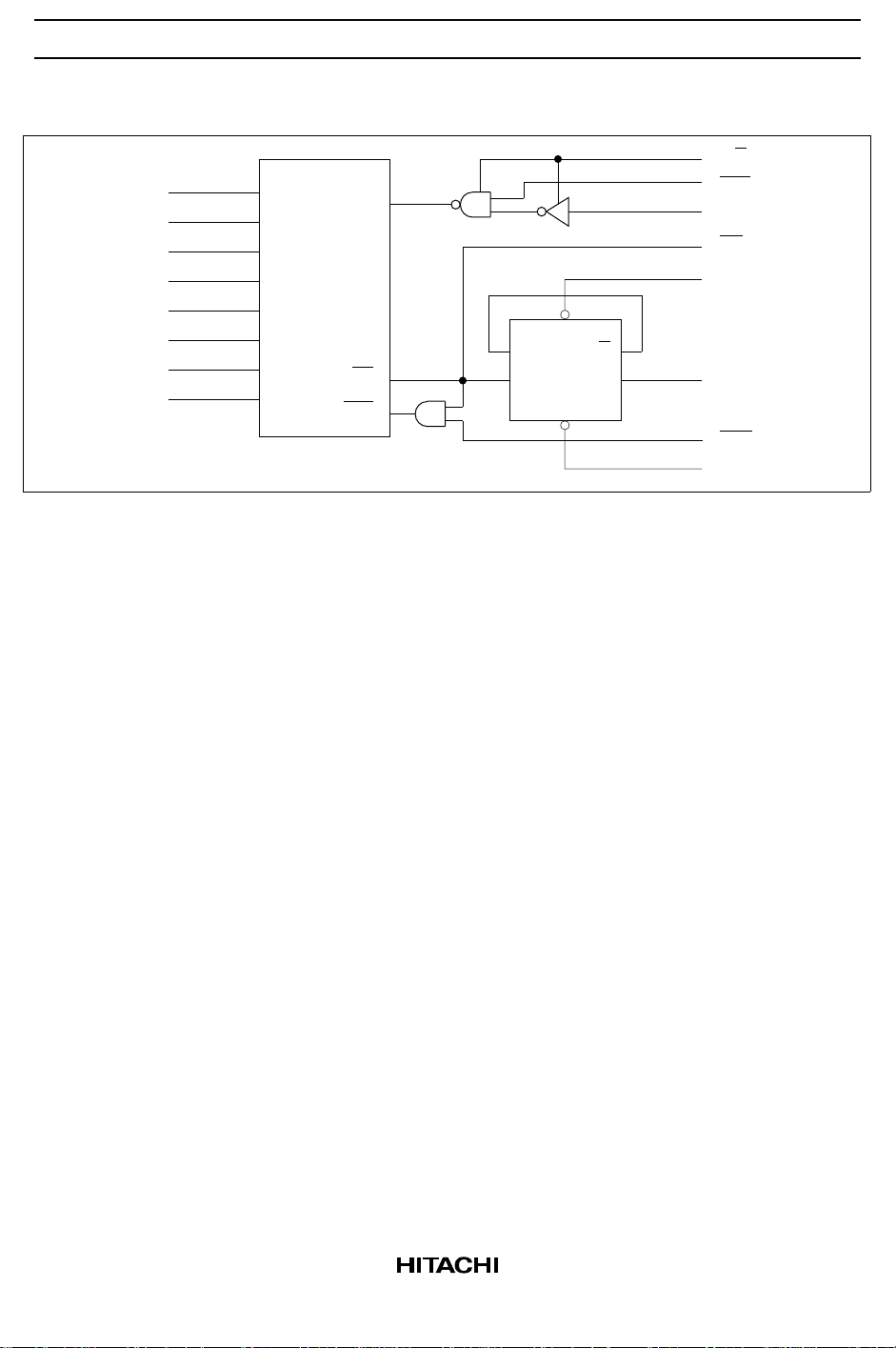
Logic Diagram
J0 J0
J1 J1
J2 J2
J3 J3
J4 J4
J5 J5
J6 J6
J7 J7
CLK
BCD decimal counter
CO
SPE
D
CK
PR
CLR
HD151011
C/T
CLK
CLK
CO
PR
Q
Q
Q
SPE
CLR
5
 Loading...