HIT HD66725A03TA0L, HD66724RA03TA0L, HCD66725A03BP, HCD66724RA03BP Datasheet

1
HD66724/HD66725
(Graphics LCD Controller/Driver
with Key Scan Function)
ADE-207-309(Z)
Rev 1.2
'99.8
Description
The HD66724/HD66725, dot-matrix graphics LCD controller and driver LSI incorporating a key scan
function up to a 4-by-8 key matrix, display characters such as alphanumerics, katakana, hiragana and
symbols as well as graphics such as kanji and pictograms. They can be configured to drive a dot-matrix
liquid crystal display and control key scan functions under the control of the microprocessor connected via
the clock-synchronized serial or 4/8-bit bus. The HD66724 is capable of displaying up to three 12character lines, 72-by-24 dot graphics and 144 segments. The HD66725 is capable of displaying up to
three 16-character lines, 96-by-24 dot graphics and 192 segments. Of the 144 (192) segments displayed, 48
(64) segments can be grayscaled. The HD66724/HD66725 have a smooth horizontal/vertical scroll display
and double-height display so that the user can easily see a variety of information within a small LCM.
The HD66724/HD66725 have various functions to reduce the power consumption of an LCD system such
as low-voltage operation of 1.8 V or less, a booster to generate maximum triple LCD drive voltage from the
supplied voltage, and voltage-followers to decrease the direct current flow in the LCD drive bleederresistors. Combining these hardware functions with software functions such as standby and sleep modes
allows fine power control. The HD66724/HD66725 are suitable for any portable battery-driven product
requiring long-term driving capabilities and small physical dimensions such as cellular phones, pagers,
portable audio devices, or electronic wallets.
Features
• Control and drive of a character and graphics LCD with built-in key scan functions
• Three 12- (16-) character lines, 72 (96) -by-24 dot graphics, and 144 (192) segments
• 48 (64) grayscale segments
• Control up to a 4 × 8 (32 key) matrix key scan.
• 3 general ports built-in
• Low-power operation support:

HD66724/HD66725
2
Vcc = 1.8 to 5.5 V (low voltage)
V
LCD
= 3.0 to 6.5 V (liquid crystal drive voltage)
Single, double or triple booster for liquid crystal drive voltage
Contrast adjuster and voltage followers to decrease direct current flow in the LCD drive bleeder-
resistors
Wake-up feature using key scan interrupt
Programmable drive duty ratios and bias values displayed on LCD
• Clock-synchronized serial interface
• 4-/8-bit bus interface capability (except when key scan circuit is used)
• 80 × 8-bit display data RAM (80 characters max)
• 20,736-bit (6 × 8 dots : 432 characters) character generator ROM
• 384 × 8-bit (64 characters) character generator RAM
• 96 × 2-bit (192 segment-icons and marks max) segment RAM
• 72- (96-) segment × 26-common-signal liquid crystal display driver
• Programmable display sizes and duty ratios
• Vertical and horizontal smooth scrolls
• Vertical double-height display
• Selectable CGROM memory bank (max. 432 fonts)
• Wide range of instruction functions:
Clear display, display on/off control, icon and mark control, character blink, black-white reversed
blinking cursor, return home, cursor on/off, black-white reversed raster-row
• No wait time for instruction execution and RAM access (zero instruction)
• Internal oscillation (with external or built-in resistor) hardware reset
• Shift change of segment and common driver
• Slim chip with bumps for chip-on-glass (COG) mounting, and tape carrier package (TCP)
Table 1 Progammable Display Sizes and Duty Ratios
Character Display Graphics Display
Duty
Ratio
Optimum
Drive Bias HD66724 HD66725 HD66724 HD66725
Segment
Display
Scanned
Keys
General
Ports
1/2 1/2 Unavailable Unavailable Unavailable Unavailable 32 (4 x 8) 3
1/10 1/4 1 line x 12
characters
1 line x 16
characters
72 x 8 dots 96 x 8 dots HD66724:
144
1/18 1/5 2 lines x 12
characters
2 lines x 16
characters
72 x 16 dots 96 x 16 dots HD66725:
192
1/26 1/6 3 lines x 12
characters
3 lines x 16
characters
72 x 24 dots 96 x 24 dots

HD66724/HD66725
3
Total Current Consumption Characteristics (Vcc = 3 V, fosc = 32 kHz, TYP
Conditions, LCD Drive Power Current Included)
Total Power Consumption
Normal Display Operation
Character
Display Size
Duty
Ratio
Optimum
Drive Bias
Frame
Frequency
Internal
Logic
LCD
Power Total*
Sleep
Mode
Standby
Mode
Segment only 1/2 1/2 80 Hz (14 µA) (12 µA) (26 µA) (11 µA) 0.1 µA
1-line display 1/10 1/4 80 Hz (20 µA) (17 µA) (54 µA) (11 µA)
2-line display 1/18 1/5 74 Hz (20 µA) (17 µA) (54 µA) (11 µA)
3-line display 1/26 1/6 77 Hz (20 µA) (17 µA) (54 µA) (11 µA)
Note : When duty ratio = 1/2 and a double booster is not used:
the total power consumption = Internal logic current + LCD power current
When duty ratio = 1/10 and a double booster is used:
the total power consumption = Internal logic current + LCD power current x 2
Type Name
Types
External
Dimensions
Operation
Voltages Internal Fonts
HD66724RA03TA0L TCP 1.8 V to 5.5 V Katakana, alphanumerics, symbols
HCD66724RA03BP Au-bumped chip and European fonts
HD66725A03TA0L TCP
HCD66725A03BP Au-bumped chip

HD66724/HD66725
4
LCD-II Family Comparison
Items HD66712U HD66720 HD66705U
Character display sizes 12 characters x 4 lines 8 characters x 2 lines 12 characters x 2 lines
Graphic display sizes — — —
Multiplexing icons 60 42 40
Annunciator — — Static: 10
Key scan control — 5 x 6 —
LED control ports — 2 —
General output port — — —
Operating power voltages 2.7 V to 5.5 V 2.7 V to 5.5 V 2.4 V to 5.5 V
Liquid crystal drive voltages 3 V to 13 V 3 V to 11 V 3 V to 9 V
Serial bus Clock-synchronized serial Clock-synchronized serial Clock-synchronized serial
Parallel bus 4 bits, 8 bits — 4 bits, 8 bits
Expansion driver control Possible Possible Impossible
Liquid crystal drive duty ratios 1/17, 33 1/9, 17 1/10, 18
Liquid crystal drive biases 1/4 to 1/6, 7 1/4 to 1/5 1/4
Liquid crystal drive waveforms B B B
Liquid crystal voltage booster Double or triple Double or triple Double or triple
Bleeder-resistor for liquid crystal drive External External Incorporated (external)
Liquid crystal drive operational amplifier — — Incorporated
Liquid crystal contrast adjuster — — Incorporated
Horizontal smooth scroll Dot unit Dot unit —
Vertical smooth scroll — — Line unit
Double-height display — — Yes
DDRAM 80 x 8 40 x 8 60 x 8
CGROM 9,600 9,600 9,600
CGRAM 64 x 8 64 x 8 32 x 5
SEGRAM 16 x 8 16 x 8 8 x 5
No. of CGROM fonts 240 240 240
No. of CGRAM fonts 8 8 4
Font sizes 5 x 8 5 x 8 5 x 8
Bit map area — — —
R-C oscillation resistor/oscillation
frequency
External resistor (270 kHz) External resistor (150 kHz) External resistor
(40, 80 kHz)
Reset function Incorporated, external Incorporated, external External
Low power control LP display mode LP display mode
Simple standby
Partial display off
Display off
Oscillation off
Liquid crystal power off
SEG/COM direction switching — — SEG only
QFP package (S mask) QFP-1420 —
TQFP package — TQFP-1414 —
TCP package TCP-128 — TCP-153
Bare chip Yes Yes Yes
Bumped chip Yes — Yes
No. of pins 128 100 153
Chip sizes 4.95 x 5.27 5.60 x 6.00 9.69 x 2.73
Pad intervals 128 µm 160 µm 120 µm

HD66724/HD66725
5
LCD-II Family Comparison (cont)
Items HD66717 HD66727 HD66724
Character display sizes 12 characters x 4 lines 12 characters x 4 lines 12 characters x 3 lines
Graphic display sizes — — 72 x 26 dots
Multiplexing icons 40 40 144
Annunciator Static: 10 Static: 12 1/2 duty: 144
Key scan control — 4 x 8 8 x 4
LED control ports — 3 —
General output ports — 3 3
Operating power voltages 2.4 V to 5.5 V 2.4 V to 5.5 V 1.8 V to 5.5 V
Liquid crystal drive voltages 3 V to 13 V 3 V to 13 V 3 V to 6 V
Serial bus I2C, Clock-synchronized
serial
I2C, Clock-synchronized
serial
Clock-synchronized serial
Parallel bus 4 bits, 8 bits — 4 bits, 8 bits
Expansion driver control Impossible Impossible Impossible
Liquid crystal drive duty ratios 1/10, 18, 26, 34 1/10, 18, 26, 34 1/2, 10, 18, 26
Liquid crystal drive biases 1/4, 1/6 1/4, 1/6 1/4 to 1/6.5
Liquid crystal drive waveforms B B B
Liquid crystal voltage booster Double or triple Double or triple Single, double or triple
Bleeder-resistor for liquid crystal drive Incorporated (external) Incorporated (external) Incorporated (external)
Liquid crystal drive operational amplifier Incorporated Incorporated Incorporated
Liquid crystal contrast adjuster Incorporated Incorporated Incorporated
Horizontal smooth scroll — — 3-dot unit
Vertical smooth scroll Line unit Line unit Line unit
Double-height display Yes Yes Yes
DDRAM 60 x 8 60 x 8 80 x 8
CGROM 9,600 11,520 20,736
CGRAM 32 x 5 32 x 6 384 x 8
SEGRAM 8 x 5 8 x 6 72 x 8
No. of CGROM fonts 240 240 240 + 192
No. of CGRAM fonts 4 4 64
Font sizes 5 x 8 5 x 8, 6 x 8 6 x 8
Bit map area — — 72 x 26
R-C oscillation resistor/
oscillation frequency
External resistor
(40-160 kHz)
External resistor
(40-160 kHz)
External resistor,
incorporated (32 kHz)
Reset function External External External
Low power control Partial display off
Display off
Oscillation off
Liquid crystal power off
Partial display off
Display off
Oscillation off
Liquid crystal power off
Key wake-up interrupt
Partial display off
Display off
Oscillation off
Liquid crystal power off
Key wake-up interrupt
SEG/COM direction switching SEG only SEG, COM SEG, COM
QFP package — — —
TQFP package — — —
TCP package TCP-153 TCP-158 TCP-146
Bare chip Yes Yes —
Bumped chip Yes Yes Yes
No. of pins 153 158 146
Chip sizes 10.88 x 2.89 11.39 x 2.89 10.34 x 2.51
Pad intervals 120 µm 120 µm 80 µm

HD66724/HD66725
6
LCD-II Family Comparison (cont)
Items HD66725 HD66726 HD66730
Character display sizes 16 characters x 3 lines 16 characters x 5 lines 6 (12) characters x 2 lines
Graphic display sizes 96 x 26 dots 96 x 42 dots —
Multiplexing icons 192 192 71
Annunciator 1/2 duty: 192 1/2 duty: 192 —
Key scan control 8 x 4 8 x 4 —
LED control ports — — —
General output ports 3 3 —
Operating power voltages 1.8 V to 5.5 V 1.8 V to 5.5 V 2.4 V to 5.5 V
Liquid crystal drive voltages 3 V to 6 V 4.0 V to 13 V 3 V to 15 V
Serial bus Clock-synchronized serial Clock-synchronized serial Clock-synchronized serial
Parallel bus 4 bits, 8 bits 4 bits, 8 bits 8 bits
Expansion driver control Impossible Impossible Possible
Liquid crystal drive duty ratios 1/2, 10, 18, 26 1/2, 10, 18, 26, 34, 42 1/14, 27, 40, 53
Liquid crystal drive biases 1/4 to 1/6.5 1/2 to 1/8 1/4 to 1/8.3
Liquid crystal drive waveforms B B B
Liquid crystal voltage booster Single, double, or triple Single, double, triple, or
quadruple
Double or triple
Bleeder-resistor for liquid crystal drive Incorporated (external) Incorporated (external) External
Liquid crystal drive operational amplifier Incorporated Incorporated —
Liquid crystal contrast adjuster Incorporated Incorporated —
Horizontal smooth scroll 3-dot unit 3-dot unit Display unit
Vertical smooth scroll Line unit Line unit Line unit
Double-height display Yes Yes —
DDRAM 80 x 8 80 x 8 80 x 8
CGROM 20,736 20,736 506,880 + 9,216
CGRAM 384 x 8 480 x 8 32 x 6
SEGRAM 96 x 8 96 x 8 8 x 6
No. of CGROM fonts 240 + 192 240 + 192 3,840
No. of CGRAM fonts 64 64 8
Font sizes 6 x 8 6 x 8 11 x 12
Bit map areas 96 x 26 96 x 42 —
R-C oscillation resistor/
oscillation frequency
External resistor,
incorporated (32 kHz)
External resistor (50 kHz) External resistor
(70–450 kHz)
Reset function External External External
Low power control Partial display off
Display off
Oscillation off
Liquid crystal power off
Key wake-up interrupt
Partial display off
Display off
Oscillation off
Liquid crystal power off
Key wake-up interrupt
Booster off
Internal division function
SEG/COM direction switching SEG, COM SEG, COM —
QFP package — — QFP-1420
TQFP package — — —
TCP package TCP-170 TCP-188 —
Bare chip — — Yes
Bumped chip Yes Yes —
No. of pins 170 188 128
Chip sizes 10.97 x 2.51 13.13 x 2.51 7.48 x 6.46
Pad intervals 80 µm 80 µm 180 µm

HD66724/HD66725
7
LCD-II Family Comparison (cont)
Items HD66731
Character display sizes 10 (20) characters x 4 lines
Graphic display sizes —
Multiplexing icons 120
Annunciator —
Key scan control —
LED control ports —
General output ports —
Operating power voltages 2.4 V to 5.5 V
Liquid crystal drive voltages 3 V to 15 V
Serial bus Clock-synchronized serial
Parallel bus 8 bits
Expansion driver control Possible
Liquid crystal drive duty ratios 1/14, 27, 40, 53
Liquid crystal drive biases 1/4 to 1/8.3
Liquid crystal drive waveforms B
Liquid crystal voltage booster Double or triple
Bleeder-resistor for liquid crystal drive External
Liquid crystal drive operational amplifier —
Liquid crystal contrast adjuster —
Horizontal smooth scroll Display unit
Vertical smooth scroll Line unit
Double-height display —
DDRAM 80 x 8
CGROM 506,880 + 9,216
CGRAM 32 x 6
SEGRAM 8 x 6
No. of CGROM fonts 3,840
No. of CGRAM fonts 8
Font sizes 11 x 12
Bit map areas —
R-C oscillation resistor/
oscillation frequency
External resistor
(70–450 kHz)
Reset function External
Low power control Booster off
Internal division function
SEG/COM direction switching —
QFP package —
TQFP package —
TCP package TCP-170, 206
Bare chip —
Bumped chip Yes
No. of pins 206
Chip sizes 7.48 x 6.46
Pad intervals 80 µm
HD66724/HD66725
8
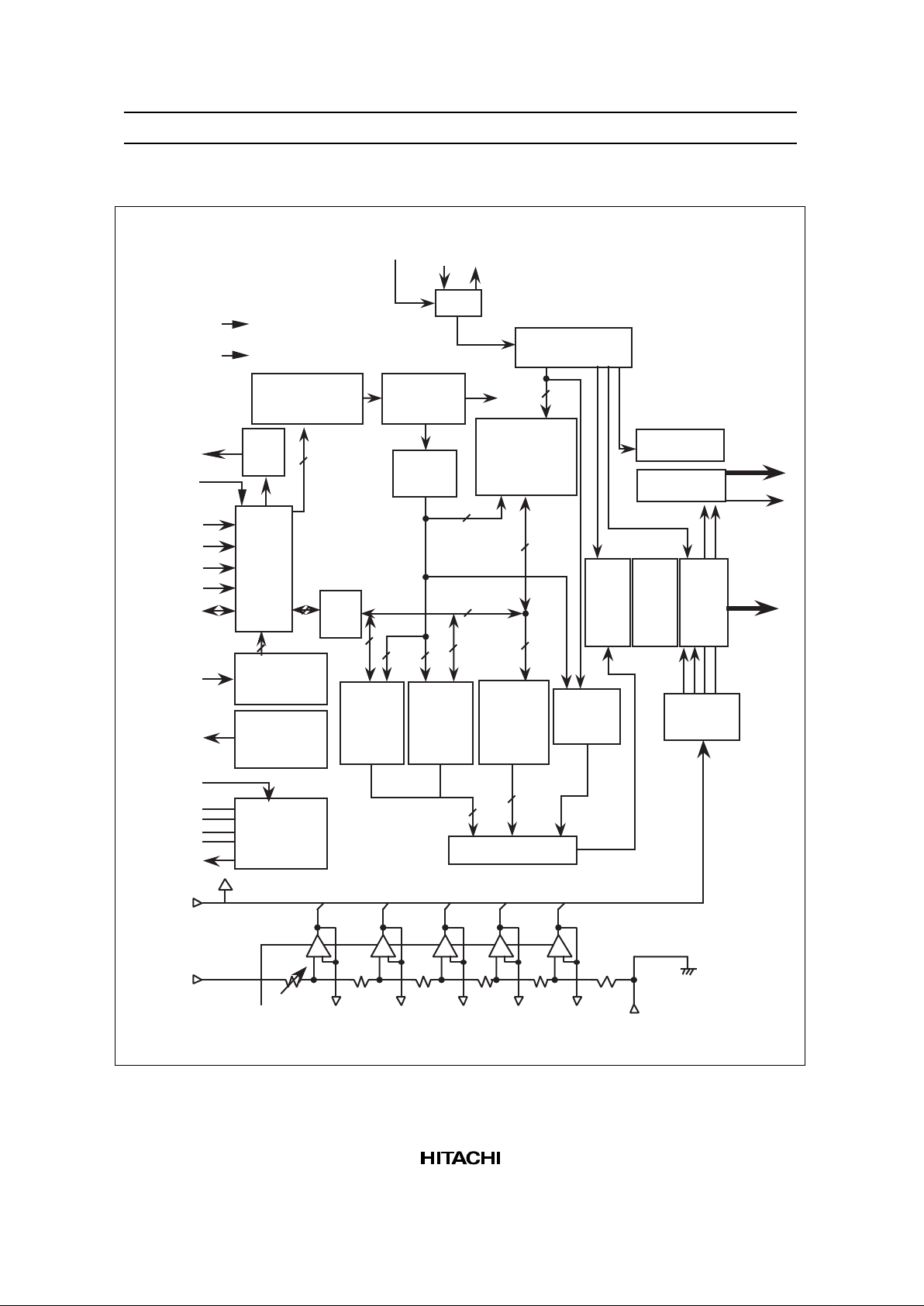
HD66724/HD66725 Block Diagram
System
interface
• Clock
synchronized
serial
• 4-bit bus
• 8-bit bus
Data
register
(DR)
Instruction register
(IR)
Address
counter
(AC)
Timing generator
Display data
RAM
(DDRAM)
80 bytes
Character
generator
RAM
(CGRAM)
384 bytes
Character
generator
ROM
(CGROM)
20,736 bits
Parallel/serial converter
Latch
circuit
Segment
shift
register
Segment
driver
LCD drive
voltage
selector
Cursor and
blink
controller
CPG
Instruction
decoder
CS*
RW/RD*/SDA
RS
E/WR*/SCL
Vcc
COM1/24–
COM24/1
SEG1/72 (96)–
SEG72 (96)/1
OSC1
R1-R3
OSC2
8
8
6
10
8
7
7
8
8
6
6
Vci
Double/triple
booster
C1+
8
7
Segmemt
RAM
(SGRAM)
24 bytes
IM2–1
RESET*
C1–
C2+
C2–
VLOUT
+- +- +- +- +-
GND
COMS1/2,
COMS2/1
VR
RRR
0
R
V
LCD
R
TEST
V1OUT V2OUT V3OUT V4OUT V5OUT
OPOFF
IM0/ID
Key scan
timing
controller
Key scan
registers
(SCAN0–SCAN3)
DB0/KIN0–
DB7/KIN7
KST0–
KST3
8
Common
driver
26-bit bidirectional
common shift register
General
output
port
PORT0 –
PORT2
HD66724/HD66725
9
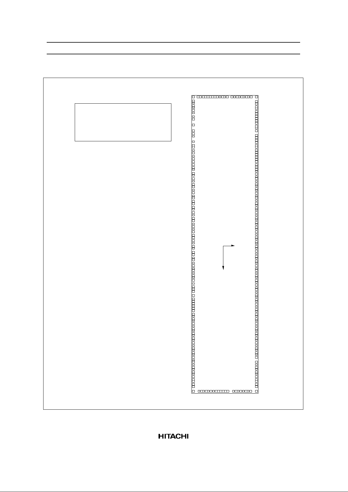
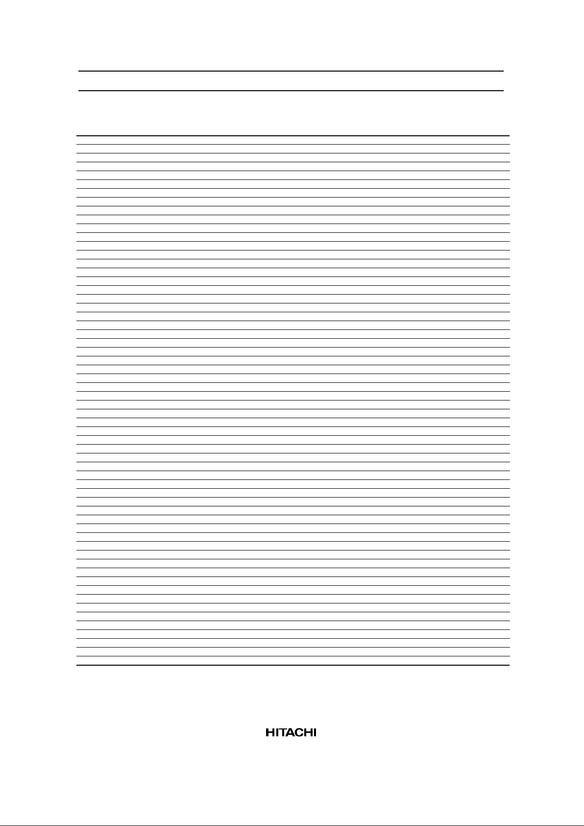
HD66724 Pad Arrangement
• Chip size: 10.34 x 2.51 mm
• Pad coordinate: Pad center
• Coordinate origin: Chip center
• Au bump size: 50 µm x 100 µm
• Au bump pitch: 80 µm (min.)
Top view
HD66724
SEG16/57
SEG15/58
SEG14/59
SEG13/60
SEG12/61
SEG11/62
SEG10/63
SEG9/64
SEG8/65
SEG7/66
SEG6/67
SEG5/68
SEG4/69
SEG3/70
SEG2/71
SEG26/47
SEG25/48
SEG24/49
SEG23/50
SEG22/51
SEG21/52
SEG20/53
SEG19/54
SEG18/55
SEG36/37
SEG35/38
SEG34/39
SEG33/40
SEG32/41
SEG31/42
SEG30/43
SEG29/44
SEG28/45
SEG27/46
SEG42/31
SEG41/32
SEG40/33
SEG39/34
SEG38/35
SEG37/36
SEG43/30
SEG17/56
SEG1/72
SEG44/29
SEG45/28
SEG46/27
SEG47/26
SEG48/25
SEG49/24
SEG50/23
SEG51/22
SEG52/21
SEG53/20
SEG54/19
SEG55/18
SEG56/17
SEG57/16
SEG58/15
SEG59/14
SEG60/13
COMS1/S2
COM1/24
COM2/23
COM3/22
COM4/21
COM5/20
COM6/19
COM8/17
OSC2
OSC1
Vcc
COM7/18
Vci
Dummy41
Dummy31
C1+
Y
X
COM20/5
COM19/6
COM18/7
SEG61/12
SEG62/11
SEG63/10
SEG64/9
SEG65/8
SEG66/7
SEG67/6
SEG68/5
SEG69/4
SEG70/3
SEG71/2
SEG72/1
C1+
C1+
C2-
C2-
C2+
C2+
Vci
Vci
Vcc
Vcc
GND
GND
GND
DB0/KIN0
DB1/KIN1
DB2/KIN2
DB3/KIN3
DB4/KIN4
DB5/KIN5
DB6/KIN6
DB7/KIN7
KST0
KST1
KST2
KST3
IRQ*
R1
R2
R3
COM17/8
RW/RD*/SDA
E/WR*/SCL
CS*
RESET*
PORT0
PORT1
C1-
C1C1-
COM9/16
COM10/15
COM11/14
COM12/13
COM13/12
COM14/11
COM15/10
COM16/9
Dummy32
Dummy33
Dummy34
Dummy36
Dummy37
Dummy38
Dummy39
Dummy40
Dummy42
Dummy43
COMS2/S1
COM24/1
COM23/2
COM22/3
COM21/4
Dummy47
Dummy48
Dummy44
VTEST3
VTEST2
VTEST1
V5OUT
V5OUT
V4OUT
V4OUT
V3OUT
V3OUT
V2OUT
V2OUT
V1OUT
V1OUT
Dummy22
Dummy3
Dummy4
Dummy11
Dummy12
Dummy2
Dummy13
C1-
C1VLOUT
VLOUT
VLOUT
VLOUT
VLCD
VLCD
VLCD
VLCD
C2-
C2-
C1+
C1+
C2+
C2+
Vci
Vci
Vcc
Vcc
PORT2
Dummy16
Dummy15
RS
RW/RD*/SDA
GND
Dummy17
Dummy35
Dummy30
Dummy29
Dummy28
Dummy27
Dummy26
Dummy25
Dummy24
Dummy23
Dummy45
Dummy46
Dummy49
Dummy50
Dummy51
Dummy52
Dummy53
Dummy54
Dummy55
Dummy56
Dummy57
Dummy58
Dummy59
Dummy1
Vcc
GND
GND
GND
GND
E/WR*/SCL
RS
CS*
RESET*
DB0/KIN0
DB1/KIN1
DB2/KIN2
DB3/KIN3
DB4/KIN4
DB5/KIN5
DB6/KIN6
DB7/KIN7
KST0
KST1
KST2
KST3
IRQ*
PORT0
PORT1
PORT2
GNDDUM
IM2
IM1
IM0/ID
VccDUM
OPOFF
TEST
Dummy8
Dummy9
Dummy10
Dummy5
Dummy6
Dummy7
Dummy14
Dummy18
Dummy19
Dummy20
Dummy21
2
HD66724/HD66725
10
HD66724 Pad Coordinates
No. Pad Name X Y No. Pad Name X Y No. Pad Name X Y No. Pad Name X Y No. Pad Name X Y
– Dummy15 –4994 –1079 50 GND 564 –1079 104 V3OUT 4915 –469 142 SEG18/55 1572 999 – Dummy41 –2863 999
– Dummy16 –4771 –1079 51 GND 644 –1079 105 V3OUT 4915 –389 143 SEG19/54 1492 999 – Dummy42 –2943 999
– Dummy17 –4690 –1079 52 GND 725 –1079 106 V4OUT 4915 –308 144 SEG20/53 1411 999 – Dummy43 –3024 999
– Dummy18 –4610 –1079 53 GND 806 –1079 107 V4OUT 4915 –227 145 SEG21/52 1331 999 – Dummy44 –3105 999
– Dummy19 –4529 –1079 54 GND 886 –1079 108 V5OUT 4915 –147 146 SEG22/51 1250 999 – Dummy45 –3185 999
– Dummy20 –4449 –1079 55 GND 967 –1079 109 V5OUT 4915 –66 147 SEG23/50 1169 999 – Dummy46 –3266 999
– Dummy21 –4368 –1079 56 GND 1048 –1079 110 VTEST1 4915 15 148 SEG24/49 1089 999 197 COMS2/S1 –3347 999
1 GNDDUM –4207 –1079 57 GND 1128 –1079 111 VTEST2 4915 95 149 SEG25/48 1008 999 198 COM24/1 –3427 999
2 IM2 –4126 –1079 58 OSC2 1209 –1079 112 VTEST3 4915 176 150 SEG26/47 927 999 199 COM23/2 –3508 999
3 IM1 –3942 –1079 59 R3 1364 –994 113 COM9/16 4915 282 151 SEG27/46 847 999 200 COM22/3 –3588 999
4 IM0/ID –3758 –1079 60 R2 1445 –994 114 COM10/15 4915 363 152 SEG28/45 766 999 201 COM21/4 –3669 999
5 VccDUM –3655 –1079 61 R1 1525 –994 115 COM11/14 4915 444 153 SEG29/44 685 999 – Dummy47 –3830 1079
6 OPOFF –3574 –1079 62 OSC1 1680 –1079 116 COM12/13 4915 524 154 SEG30/43 605 999 – Dummy48 –3911 1079
7 TEST –3390 –1079 63 Vcc 1783 –1079 117 COM13/12 4915 605 155 SEG31/42 524 999 – Dummy49 –3992 1079
8 PORT2 –3287 –1079 64 Vcc 1864 –1079 118 COM14/11 4915 685 156 SEG32/41 444 999 – Dummy50 –4072 1079
9 PORT2 –3206 –1079 65 Vcc 1945 –1079 119 COM15/10 4915 766 157 SEG33/40 363 999 – Dummy51 –4153 1079
10 PORT1 –3103 –1079 66 Vcc 2025 –1079 120 COM16/9 4915 847 158 SEG34/39 282 999 – Dummy52 –4234 1079
11 PORT1 –3022 –1079 67 Vcc 2106 –1079 – Dummy23 4915 1079 159 SEG35/38 202 999 – Dummy53 –4314 1079
12 PORT0 –2919 –1079 68 Vcc 2187 –1079 – Dummy24 4717 1079 160 SEG36/37 121 999 – Dummy54 –4395 1079
13 PORT0 –2838 –1079 69 Vci 2290 –999 – Dummy25 4637 1079 161 SEG37/36 40 999 – Dummy55 –4476 1079
14 IRQ* –2735 –1079 70 Vci 2371 –999 – Dummy26 4556 1079 162 SEG38/35 –40 999 – Dummy56 –4556 1079
15 IRQ* –2654 –1079 71 Vci 2451 –999 – Dummy27 4476 1079 163 SEG39/34 –121 999 – Dummy57 –4637 1079
16 KST3 –2551 –1079 72 Vci 2532 –999 – Dummy28 4395 1079 164 SEG40/33 –202 999 – Dummy58 –4717 1079
17 KST3 –2470 –1079 73 Vci 2613 –999 – Dummy29 4314 1079 165 SEG41/32 –282 999 – Dummy59 –4798 1079
18 KST2 –2367 –1079 74 C2+ 2693 –999 – Dummy30 4234 1079 166 SEG42/31 –363 999 – Dummy1 –4994 1079
19 KST2 –2286 –1079 75 C2+ 2774 –999 – Dummy31 4153 1079 167 SEG43/30 –444 999 202 COM8/17 –4915 847
20 KST1 –2183 –1079 76 C2+ 2854 –999 – Dummy32 4072 1079 168 SEG44/29 –524 999 203 COM7/18 –4915 766
21 KST1 –2102 –1079 77 C2+ 2935 –999 – Dummy33 3992 1079 169 SEG45/28 –605 999 204 COM6/19 –4915 685
22 KST0 –1999 –1079 78 C2– 3016 –999 – Dummy34 3911 1079 170 SEG46/27 –685 999 205 COM5/20 –4915 605
23 KST0 –1918 –1079 79 C2– 3096 –999 121 COM17/8 3750 999 171 SEG47/26 –766 999 206 COM4/21 –4915 524
24 DB7/KIN7 –1815 –1079 80 C2– 3177 –999 122 COM18/7 3669 999 172 SEG48/25 –847 999 207 COM3/22 –4915 444
25 DB7/KIN7 –1734 –1079 81 C2– 3258 –999 123 COM19/6 3588 999 173 SEG49/24 –927 999 208 COM2/23 –4915 363
26 DB6/KIN6 –1631 –1079 82 C1+ 3338 –999 124 COM20/5 3508 999 174 SEG50/23 –1008 999 209 COM1/24 –4915 282
27 DB6/KIN6 –1551 –1079 83 C1+ 3419 –999 – Dummy35 3427 999 175 SEG51/22 –1089 999 210 COMS1/S2 –4915 202
28 DB5/KIN5 –1447 –1079 84 C1+ 3500 –999 – Dummy36 3347 999 176 SEG52/21 –1169 999 – Dummy2 –4994 50
29 DB5/KIN5 –1367 –1079 85 C1+ 3580 –999 – Dummy37 3266 999 177 SEG53/20 –1250 999 – Dummy3 –4994 –30
30 DB4/KIN4 –1263 –1079 86 C1+ 3661 –999 – Dummy38 3185 999 178 SEG54/19 –1331 999 – Dummy4 –4994 –111
31 DB4/KIN4 –1183 –1079 87 C1– 3741 –999 – Dummy39 3105 999 179 SEG55/18 –1411 999 – Dummy5 –4994 –192
32 DB3/KIN3 –1079 –1079 88 C1– 3822 –999 – Dummy40 3024 999 180 SEG56/17 –1492 999 – Dummy6 –4994 –272
33 DB3/KIN3 –999 –1079 89 C1– 3903 –999 125 SEG1/72 2943 999 181 SEG57/16 –1572 999 – Dummy7 –4994 –353
34 DB2/KIN2 –895 –1079 90 C1– 3983 –999 126 SEG2/71 2863 999 182 SEG58/15 –1653 999 – Dummy8 –4994 –433
35 DB2/KIN2 –815 –1079 91 C1– 4064 –999 127 SEG3/70 2782 999 183 SEG59/14 –1734 999 – Dummy9 –4994 –514
36 DB1/KIN1 –711 –1079 92 VLOUT 4145 –999 128 SEG4/69 2701 999 184 SEG60/13 –1814 999 – Dummy10 –4994 –595
37 DB1/KIN1 –631 –1079 93 VLOUT 4225 –999 129 SEG5/68 2621 999 185 SEG61/12 –1895 999 – Dummy11 –4994 –675
38 DB0/KIN0 –527 –1079 94 VLOUT 4306 –999 130 SEG6/67 2540 999 186 SEG62/11 –1976 999 – Dummy12 –4994 –756
39 DB0/KIN0 –447 –1079 95 VLOUT 4387 –999 131 SEG7/66 2460 999 187 SEG63/10 –2056 999 – Dummy13 –4994 –837
40 RESET* –343 –1079 96 VLCD 4467 –999 132 SEG8/65 2379 999 188 SEG64/9 –2137 999 – Dummy14 –4994 –917
41 RESET* –263 –1079 97 VLCD 4548 –999 133 SEG9/64 2298 999 189 SEG65/8 –2218 999
42 CS* –159 –1079 98 VLCD 4629 –999 134 SEG10/63 2218 999 190 SEG66/7 –2298 999
43 CS* –79 –1079 99 VLCD 4709 –999 135 SEG11/62 2137 999 191 SEG67/6 –2379 999
44 RS 24 –1079 – Dummy22 4915 –1079 136 SEG12/61 2056 999 192 SEG68/5 –2460 999
45 RS 105 –1079 100 V1OUT 4915 –792 137 SEG13/60 1976 999 193 SEG69/4 –2540 999
46 E/WR*/SCL 198 –1079 101 V1OUT 4915 –711 138 SEG14/59 1895 999 194 SEG70/3 –2621 999
47 E/WR*/SCL 279 –1079 102 V2OUT 4915 –631 139 SEG15/58 1814 999 195 SEG71/2 –2701 999
48 RW/RD*/SDA 368 –1079 103 V2OUT 4915 –550 140 SEG16/57 1734 999 196 SEG72/1 –2782 999
49 RW/RD*/SDA 449 –1079 141 SEG17/56 1653 999
HD66724/HD66725
11
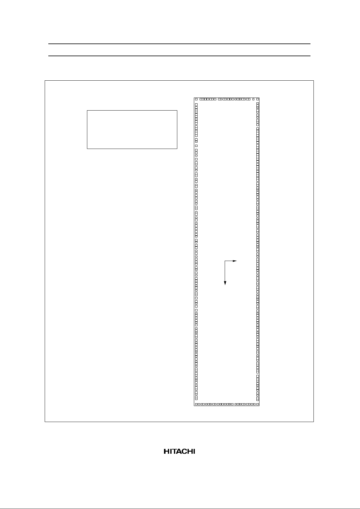
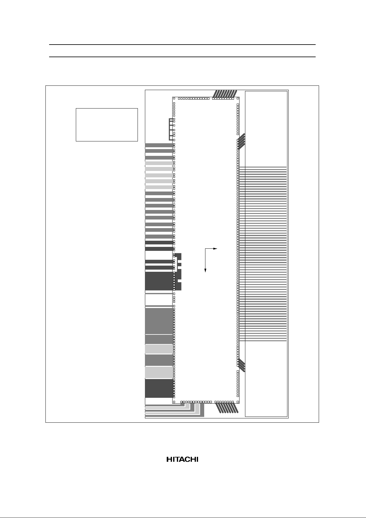
HD66725 Pad Arrangement
• Chip size: 10.97 x 2.51 mm
• Pad coordinates: Pad center
• Coordinate origin: Chip center
• Au bump size: 50 µm x 100 µm
• Au bump pitch: 80 µm (min.)
(Top view)
HD66725
SEG16/81
SEG15/82
SEG14/83
SEG13/84
SEG12/85
SEG11/86
SEG10/87
SEG9/64
SEG8/89
SEG7/90
SEG6/91
SEG5/92
SEG4/93
SEG3/94
SEG2/95
SEG26/71
SEG25/72
SEG24/73
SEG23/74
SEG22/75
SEG21/76
SEG20/77
SEG19/78
SEG18/79
SEG36/61
SEG35/62
SEG34/63
SEG33/64
SEG32/65
SEG31/66
SEG30/67
SEG29/68
SEG28/69
SEG27/70
SEG42/55
SEG41/56
SEG40/57
SEG39/58
SEG38/59
SEG37/60
SEG43/54
SEG17/80
SEG1/96
SEG44/53
SEG45/52
SEG46/51
SEG47/50
SEG48/49
SEG49/48
SEG50/47
SEG51/46
SEG52/45
SEG53/44
SEG54/43
SEG55/42
SEG56/41
SEG57/40
SEG58/39
SEG59/38
SEG60/37
COMS1/S2
COM1/24
COM2/23
COM3/22
COM4/21
COM5/20
COM6/19
COM8/17
OSC2
OSC1
Vcc
COM7/18
Vci
Dummy37
C1+
Y
X
COM20/5
COM19/6
COM18/7
SEG61/36
SEG62/35
SEG63/34
SEG64/33
SEG65/32
SEG66/31
SEG67/30
SEG68/29
SEG69/28
SEG70/27
SEG71/26
SEG72/25
C1+
C1+
C2-
C2-
C2+
C2+
Vci
Vci
Vcc
Vcc
GND
GND
GND
DB0/KIN0
DB1/KIN1
DB2/KIN2
DB3/KIN3
DB4/KIN4
DB5/KIN5
DB6/KIN6
DB7/KIN7
KST0
KST1
KST2
KST3
IRQ*
R1
R2
R3
COM17/8
RW/RD*/SDA
E/WR*/SCL
CS*
RESET*
PORT0
PORT1
C1-
C1C1-
COM9/16
COM10/15
COM11/14
COM12/13
COM13/12
COM14/11
COM15/10
COM16/9
Dummy38
Dummy39
Dummy40
Dummy44
Dummy45
VTEST3
VTEST2
VTEST1
V5OUT
V5OUT
V4OUT
V4OUT
V3OUT
V3OUT
V2OUT
V2OUT
V1OUT
V1OUT
Dummy25
Dummy2
C1-
C1VLOUT
VLOUT
VLOUT
VLOUT
V
LCD
V
LCD
V
LCD
V
LCD
C2-
C2-
C1+
C1+
C2+
C2+
Vci
Vci
Vcc
Vcc
PORT2
Dummy17
Dummy10
RS
RW/RD*/SDA
GND
Dummy18
Dummy43
Dummy36
Dummy35
Dummy34
Dummy33
Dummy32
Dummy31
Dummy30
Dummy29
Dummy46
Dummy47
Dummy48
Dummy49
Dummy50
Dummy51
Dummy52
Dummy53
Dummy1
Vcc
GND
GND
GND
GND
E/WR*/SCL
RS
CS*
RESET*
DB0/KIN0
DB1/KIN1
DB2/KIN2
DB3/KIN3
DB4/KIN4
DB5/KIN5
DB6/KIN6
DB7/KIN7
KST0
KST1
KST2
KST3
IRQ*
PORT0
PORT1
PORT2
GNDDUM
IM2
IM1
IM0/ID
VccDUM
OPOFF
TEST
Dummy6
Dummy7
Dummy8
Dummy3
Dummy4
Dummy5
Dummy19
Dummy20
Dummy21
Dummy22
SEG73/24
SEG74/23
SEG75/22
SEG76/21
SEG77/20
SEG78/19
SEG79/18
SEG80/17
SEG81/16
SEG82/15
SEG83/14
SEG84/13
SEG85/12
SEG86/11
SEG87/10
SEG88/9
SEG89/8
SEG90/7
SEG91/6
SEG92/5
SEG93/4
SEG94/3
SEG95/2
SEG96/1
COM21/4
COM22/3
COM23/2
COM24/1
COMS2/S1
Dummy16
Dummy15
Dummy14
Dummy13
Dummy9
Dummy12
Dummy11
Dummy54
Dummy23
Dummy24
Dummy27
Dummy26
Dummy28
Dummy42
Dummy41
2
HD66724/HD66725
12
HD66725 Pad Coordinates
No. Pad Name X Y No. Pad Name X Y No. Pad Name X Y No. Pad Name X Y No. Pad Name X Y
— Dummy10 –5309 –1079 46 E/WR*/SCL 513 –1079 103 V2OUT 5230 –550 146 SEG22/75 1726 999 206 SEG82/15 –3112 999
— Dummy11 –5101 –1079 47 E/WR*/SCL 594 –1079 104 V3OUT 5230 –469 147 SEG23/74 1646 999 207 SEG83/14 –3193 999
— Dummy12 –5021 –1079 48 RW/RD*/SDA 683 –1079 105 V3OUT 5230 –389 148 SEG24/73 1565 999 208 SEG84/13 –3273 999
— Dummy13 –4940 –1079 49 RW/RD*/SDA 764 –1079 106 V4OUT 5230 –308 149 SEG25/72 1484 999 209 SEG85/12 –3354 999
— Dummy14 –4859 –1079 50 GND 879 –1079 107 V4OUT 5230 –227 150 SEG26/71 1404 999 210 SEG86/11 –3435 999
— Dummy15 –4779 –1079 51 GND 959 –1079 108 V5OUT 5230 –147 151 SEG27/70 1323 999 211 SEG87/10 –3515 999
— Dummy16 –4698 –1079 52 GND 1040 –1079 109 V5OUT 5230 –66 152 SEG28/69 1242 999 212 SEG88/9 –3596 999
— Dummy17 –4617 –1079 53 GND 1121 –1079 110 VTEST1 5230 15 153 SEG29/68 1162 999 213 SEG89/8 –3677 999
— Dummy18 –4537 –1079 54 GND 1201 –1079 111 VTEST2 5230 95 154 SEG30/67 1081 999 214 SEG90/7 –3757 999
— Dummy19 –4456 –1079 55 GND 1282 –1079 112 VTEST3 5230 176 155 SEG31/66 1000 999 215 SEG91/6 –3838 999
— Dummy20 –4375 –1079 56 GND 1363 –1079 113 COM9/16 5230 282 156 SEG32/65 920 999 216 SEG92/5 –3919 999
— Dummy21 –4295 –1079 57 GND 1443 –1079 114 COM10/15 5230 363 157 SEG33/64 839 999 217 SEG93/4 –3999 999
— Dummy22 –4214 –1079 58 OSC2 1524 –1079 115 COM11/14 5230 444 158 SEG34/63 759 999 218 SEG94/3 –4080 999
— Dummy23 –4134 –1079 59 R3 1679 –994 116 COM12/13 5230 524 159 SEG35/62 678 999 219 SEG95/2 –4161 999
— Dummy24 –4053 –1079 60 R2 1760 –994 117 COM13/12 5230 605 160 SEG36/61 597 999 220 SEG96/1 –4241 999
1 GNDDUM –3892 –1079 61 R1 1840 –994 118 COM14/11 5230 685 161 SEG37/60 517 999 — Dummy45 –4404 1079
2 IM2 –3811 –1079 62 OSC1 1995 –1079 119 COM15/10 5230 766 162 SEG38/59 436 999 — Dummy46 –4484 1079
3 IM1 –3627 –1079 63 Vcc 2098 –1079 120 COM16/9 5230 847 163 SEG39/58 355 999 — Dummy47 –4565 1079
4 IM0/ID –3443 –1079 64 Vcc 2179 –1079 — Dummy28 5230 927 164 SEG40/57 275 999 — Dummy48 –4646 1079
5 VccDUM –3340 –1079 65 Vcc 2260 –1079 — Dummy29 5230 1079 165 SEG41/56 194 999 — Dummy49 –4726 1079
6 OPOFF –3259 –1079 66 Vcc 2340 –1079 — Dummy30 5032 1079 166 SEG42/55 113 999 — Dummy50 –4807 1079
7 TEST –3075 –1079 67 Vcc 2421 –1079 — Dummy31 4952 1079 167 SEG43/54 33 999 — Dummy51 –4888 1079
8 PORT2 –2972 –1079 68 Vcc 2502 –1079 — Dummy32 4871 1079 168 SEG44/53 –48 999 — Dummy52 –4968 1079
9 PORT2 –2891 –1079 69 Vci 2605 –999 — Dummy33 4791 1079 169 SEG45/52 –129 999 — Dummy53 –5049 1079
10 PORT1 –2788 –1079 70 Vci 2686 –999 — Dummy34 4710 1079 170 SEG46/51 –209 999 — Dummy54 –5129 1079
11 PORT1 –2707 –1079 71 Vci 2766 –999 — Dummy35 4629 1079 171 SEG47/50 –290 999 — Dummy1 –5309 1079
12 PORT0 –2604 –1079 72 Vci 2847 –999 — Dummy36 4549 1079 172 SEG48/49 –370 999 — Dummy2 –5309 955
13 PORT0 –2523 –1079 73 Vci 2928 –999 — Dummy37 4468 1079 173 SEG49/48 –451 999 221 COMS2/S1 –5229 794
14 IRQ* –2420 –1079 74 C2+ 3008 –999 — Dummy38 4387 1079 174 SEG50/47 –532 999 222 COM24/1 –5229 713
15 IRQ* –2339 –1079 75 C2+ 3089 –999 — Dummy39 4307 1079 175 SEG51/46 –612 999 223 COM23/2 –5229 633
16 KST3 –2236 –1079 76 C2+ 3169 –999 — Dummy40 4226 1079 176 SEG52/45 –693 999 224 COM22/3 –5229 552
17 KST3 –2155 –1079 77 C2+ 3250 –999 121 COM17/8 4065 999 177 SEG53/44 –774 999 225 COM21/4 –5229 471
18 KST2 –2052 –1079 78 C2– 3331 –999 122 COM18/7 3984 999 178 SEG54/43 –854 999 226 COM8/17 –5229 391
19 KST2 –1971 –1079 79 C2– 3411 –999 123 COM19/6 3903 999 179 SEG55/42 –935 999 227 COM7/18 –5229 310
20 KST1 –1868 –1079 80 C2– 3492 –999 124 COM20/5 3823 999 180 SEG56/41 –1016 999 228 COM6/19 –5229 229
21 KST1 –1787 –1079 81 C2– 3573 –999 — Dummy41 3742 999 181 SEG57/40 –1096 999 229 COM5/20 –5229 149
22 KST0 –1684 –1079 82 C1+ 3653 –999 — Dummy42 3662 999 182 SEG58/39 –1177 999 230 COM4/21 –5229 68
23 KST0 –1603 –1079 83 C1+ 3734 –999 — Dummy43 3581 999 183 SEG59/38 –1257 999 231 COM3/22 –5229 –13
24 DB7/KIN7 –1500 –1079 84 C1+ 3815 –999 — Dummy44 3500 999 184 SEG60/37 –1338 999 232 COM2/23 –5229 –93
25 DB7/KIN7 –1419 –1079 85 C1+ 3895 –999 125 SEG1/96 3420 999 185 SEG61/36 –1419 999 233 COM1/24 –5229 –174
26 DB6/KIN6 –1316 –1079 86 C1+ 3976 –999 126 SET2/95 3339 999 186 SEG62/35 –1499 999 234 COMS1/S2 –5229 –255
27 DB6/KIN6 –1236 –1079 87 C1– 4056 –999 127 SEG3/94 3258 999 187 SEG63/34 –1580 999 — Dummy3 –5309 –433
28 DB5/KIN5 –1132 –1079 88 C1– 4137 –999 128 SEG4/93 3178 999 188 SEG64/33 –1661 999 — Dummy4 –5309 –514
29 DB5/KIN5 –1052 –1079 89 C1– 4218 –999 129 SEG5/92 3097 999 189 SEG65/32 –1741 999 — Dummy5 –5309 –595
30 DB4/KIN4 –948 –1079 90 C1– 4298 –999 130 SEG6/91 3016 999 190 SEG66/31 –1822 999 — Dummy6 –5309 –675
31 DB4/KIN4 –868 –1079 91 C1– 4379 –999 131 SEG7/90 2936 999 191 SEG67/30 –1903 999 — Dummy7 –5309 –756
32 DB3/KIN3 –764 –1079 92 VLOUT 4460 –999 132 SEG8/89 2855 999 192 SEG68/29 –1983 999 — Dummy8 –5309 –837
33 DB3/KIN3 –684 –1079 93 VLOUT 4540 –999 133 SEG9/88 2775 999 193 SEG69/28 –2064 999 — Dummy9 –5309 –917
34 DB2/KIN2 –580 –1079 94 VLOUT 4621 –999 134 SEG10/87 2694 999 194 SEG70/27 –2145 999
35 DB2/KIN2 –500 –1079 95 VLOUT 4702 –999 135 SEG11/86 2613 999 195 SEG71/26 –2225 999
36 DB1/KIN1 –396 –1079 96 VLCD 4782 –999 136 SEG12/85 2533 999 196 SEG72/25 –2306 999
37 DB1/KIN1 –316 –1079 97 VLCD 4863 –999 137 SEG13/84 2452 999 197 SEG73/24 –2386 999
38 DB0/KIN0 –212 –1079 98 VLCD 4944 –999 138 SEG14/83 2371 999 198 SEG74/23 –2467 999
39 DB0/KIN0 –132 –1079 99 VLCD 5024 –999 139 SEG15/82 2291 999 199 SEG75/22 –2548 999
40 RESET* –28 –1079 — Dummy25 5230 –1079 140 SEG16/81 2210 999 200 SEG76/21 –2628 999
41 RESET* 52 –1079 — Dummy26 5230 –953 141 SEG17/80 2129 999 201 SEG77/20 –2709 999
42 CS* 156 –1079 — Dummy27 5230 –872 142 SEG18/79 2049 999 202 SEG78/19 –2790 999
43 CS* 236 –1079 100 V1OUT 5230 –792 143 SEG19/78 1968 999 203 SEG79/18 –2870 999
44 RS 339 –1079 101 V1OUT 5230 –711 144 SEG20/77 1887 999 204 SEG80/17 –2951 999
45 RS 420 –1079 102 V2OUT 5230 –631 145 SEG21/76 1807 999 205 SEG81/16 –3032 999
HD66724/HD66725
13
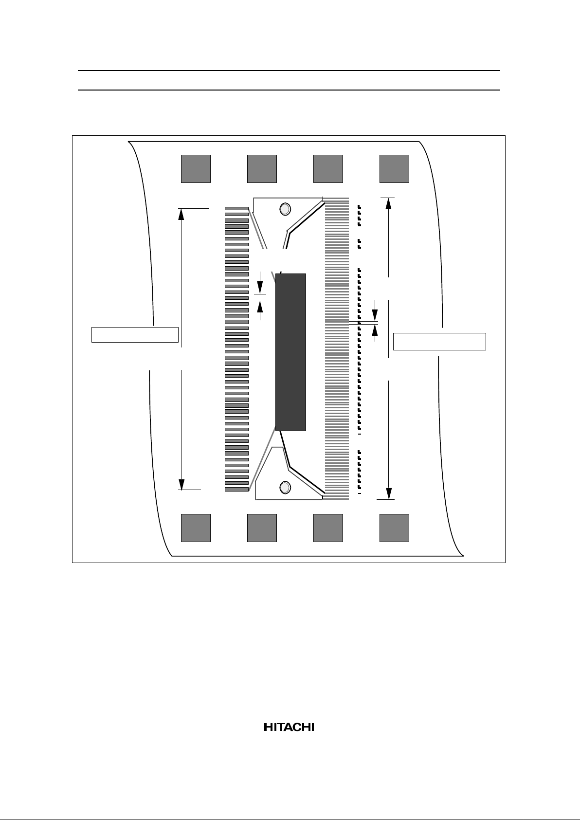
Chip-on-Glass (COG) Routing Example
COM21/4
COM22/3
COM23/2
COM24/1
COMS2/S1
SEG72/1
SEG71/2
SEG70/3
SEG69/4
SEG68/5
SEG67/6
SEG66/7
SEG65/8
SEG64/9
SEG63/10
SEG62/11
SEG61/12
SEG60/13
SEG59/14
SEG58/15
SEG57/16
SEG56/17
SEG55/18
SEG54/19
SEG53/20
SEG52/21
SEG51/22
SEG50/23
SEG49/24
SEG48/25
SEG47/26
SEG46/27
SEG45/28
SEG44/29
SEG43/30
SEG42/31
SEG41/32
SEG40/33
SEG39/34
SEG38/35
SEG37/36
SEG36/37
SEG35/38
SEG34/39
SEG33/40
SEG32/41
SEG31/42
SEG30/43
SEG29/44
SEG28/45
SEG27/46
SEG26/47
SEG25/48
SEG24/49
SEG23/50
SEG22/51
SEG21/52
SEG20/53
SEG19/54
SEG18/55
SEG17/56
SEG16/57
SEG15/58
SEG14/59
SEG13/60
SEG12/61
SEG11/62
SEG10/63
SEG9/64
SEG8/65
SEG7/66
SEG6/67
SEG5/68
SEG4/69
SEG3/70
SEG2/71
SEG1/72
COM20/5
COM19/6
COM18/7
COM17/8
IM0/ID
TEST
GNDDUM
IM2
V
CC
DUM
OPOFF
COM8/17
COM7/18
COM6/19
COM5/20
COM4/21
COM3/22
COM2/23
COM1/24
COMS1/S2
COM16/9
COM15/10
COM14/11
COM13/12
COM12/13
COM11/14
COM10/15
COM9/16
VTEST3
VTEST2
VTEST1
V5OUT
V4OUT
V3OUT
V2OUT
V1OUT
DB7/KIN7
KST2
KST3
IRQ*
PORT0
PORT1
PORT2
KST1
KST0
DB6/KIN6
DB5/KIN5
DB4/KIN4
DB3/KIN3
DB2/KIN2
DB1/KIN1
DB0/KIN0
RESET*
CS*
RS
R3
R2
R1
V
CC
V
ci
C2+
C2-
C1+
C1-
VLOUT
V
LCD
OSC1
OSC2
IM1
HD66724
(Top view)
X
Y
• Clock-synchronized serial bus
• Unused key scan
• Unused port output
• Quadruple booster
• Internal operational amplifier
E/WR*/SCL
RW/RD*/SDA
GND
HD66724/HD66725
14
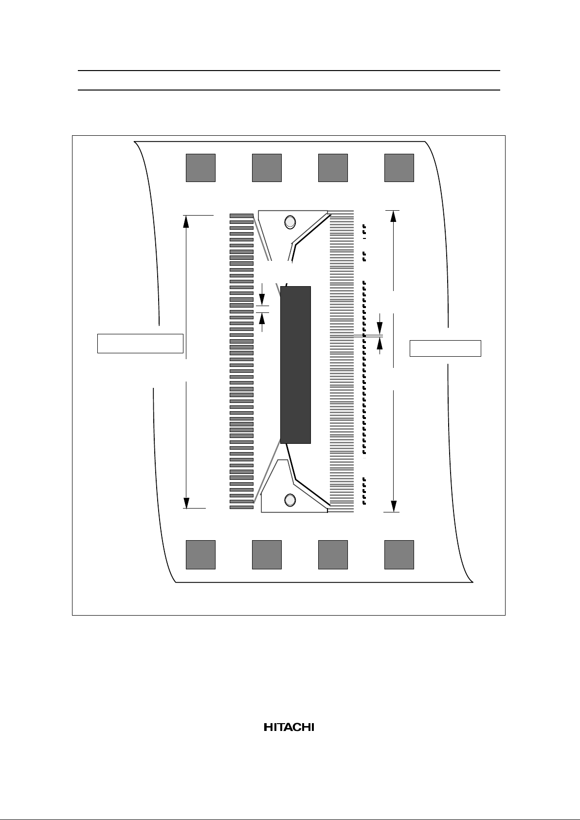
TCP Dimensions (HD66724TA0)
COMS1/S2
COM1/24
COM8/17
SEG72/1
SEG1/72
COM20/5
COM9/16
Dummy
0.50P x (48 – 1)
= 23.5 mm
0.26P x (100 – 1)
= 25.74 mm
0.26-mm
pitch
LCD Driver
I/O, Power supply
HITACHI
HITACHI
HD66724
HD66724
COM21/4
COM24/1
COMS2/S1
Dummy
IM2
IM1
IM0/ID
OPOFF
TEST
PORT2
KST3
KST2
KST1
KST0
DB7/KIN7
DB6/KIN6
DB5/KIN5
DB4/KIN4
DB3/KIN3
DB2/KIN2
DB1/KIN1
DB0/KIN0
RESET*
CS*
RS
E/WR*/SCL
RW/RD*/SDA
GND
OSC2
OSC1
Vcc
Vci
C2+
C2-
C1+
C1-
VLOUT
VLCD
V1OUT
V2OUT
V3OUT
V4OUT
V5OUT
PORT1
PORT0
IRQ*
VTEST1
VTSET2
VTEST3
R3
R2
R1
VTEST3
0.50-mm
pitch
HD66724/HD66725
15
TCP Dimensions (HD66725TA0)
COMS1/S2
COM1/24
COM8/17
SEG96/1
SEG1/96
COM20/5
COM9/16
Dummy
0.65P x (50 – 1)
= 31.85 mm
0.25P x (126 – 1)
= 31.25 mm
0.25-mm
pitch
LCD driver
Power supply, I/O
HITACHI
HITACHI
HD66725
HD66725
COM21/4
COM24/1
COMS2/S1
Dummy
IM2
IM1
IM0/ID
OPOFF
TEST
PORT2
KST3
KST2
KST1
KST0
DB7/KIN7
DB6/KIN6
DB5/KIN5
DB4/KIN4
DB3/KIN3
DB2/KIN2
DB1/KIN1
DB0/KIN0
RESET*
CS*
RS
E/WR*/SCL
RW/RD*/SDA
GND
OSC2
OSC1
Vcc
Vci
C2+
C2-
C1+
C1-
VLOUT
VLCD
V1OUT
V2OUT
V3OUT
V4OUT
V5OUT
PORT1
PORT0
IRQ*
VTEST1
VTSET2
VTEST3
R3
R2
R1
VTEST3
0.65-mm
pitch
Dummy
Dummy
NC
NC
Note: The NC pin in the input side is electrically floating.

HD66724/HD66725
16
Pin Functions
Table 2 Pin Functional Description
Signals
Number of
Pins I/O Connected to Functions
IM2, IM1 2 I V
CC
or GND Selects the MPU interface mode:
IM2
“GND”
“GND”
“Vcc”
“Vcc”
IM1
“GND”
“Vcc”
“GND”
“Vcc”
MPU interface
Clock-synchronized serial interface
68-system parallel bus interface
Setting inhibited
80-system parallel bus interface
IM0/ID 1 I V
CC
or GND Inputs the ID of the device ID code for a serial bus
interface. Selects the transfer bus width for a parallel
bus interface.
GND: 8-bit bus, Vcc: 4-bit bus
CS* 2 I MPU Selects the HD66724/HD66725:
Low: HD66724/HD66725 are selected and can be
accessed
High: HD66724/HD66725 are not selected and
cannot be accessed
Must be fixed at GND level when not in use.
RS 2 I MPU Selects the register for a parallel bus interface.
Low: Instruction High: RAM access
Selects the key scan interrupt method in the standby
period for a serial interface. Monitors a total of eight
keys connected to KST0 at the GND level and
monitors all keys at the Vcc level to generate an
interrupt. Must be fixed at the Vcc or GND level.
E/WR*/SCL 2 I MPU Inputs the serial transfer clock for a serial interface.
Fetches data at the rising edge of a clock.
For a 68-system parallel bus interface, serves as an
enable signal to activate data read/write operation.
For an 80-system parallel bus interface, serves as a
write strobe signal and writes data at the low level.
RW/RD*/
SDA
2 I/O orIMPU Serves as the bidirectional serial transfer data for a
serial interface. Sends/Receives data.
For a 68-system parallel bus interface, serves as a
signal to select data read/write operation.
For an 80-system parallel bus interface, serves as a
write strobe signal and reads data at the low level.
IRQ* 2 O MPU Generates the key scan interrupt signal.
KST0–
KST3
8 O Key matrix Generates strobe signals for latching scanned data
from the key matrix at specific time intervals.
Available for a serial interface only.
DB0/KIN0–
DB7/KIN7
16 I or
I/O
Key matrix or
MPU
Samples key state from key matrix synchronously
with strobe signals for a serial interface.
Serves as a bidirectional data bus for a parallel bus
interface.
For a four-bit bus, data transfer uses KIN7/DB7–
KIN4/DB4; leave KIN3/DB3–KIN0/DB0 disconnected.

HD66724/HD66725
17
Table 2 Pin Functional Description (cont)
Signals
Number of
Pins I/O Connected to Functions
PORT0–
PORT2
6 O General output General output ports. These ports cannot drive
current such as for LEDs or backlighting control.
Boost the current using an external transistor.
COMS1/2,
COMS2/1
2 O LCD Two common output signals for segment-icon
display.
COM1/24–
COM24/1
24 O LCD Common output signals for character/graphics
display: COM1 to COM8 for the first line; COM9 to
COM16 for the second line, and COM17 to COM24
for the third line. All the unused pins output
deselection waveforms. In the sleep mode (SLP = 1)
or standby mode (STB = 1), all pins output GND
level.
The CMS bit can change the shift direction of the
common signal. For example, if CMS = 0, COM1/24
is COM1. If CMS = 1, COM1/24 is COM24.
SEG1/72–
SEG72/1
(HD66724)
72 O LCD Segment output signals for segment-icon display and
character/graphics display. In the sleep mode (SLP =
1) or standby mode (STB = 1), all pins output GND
level.
SEG1/96–
SEG96/1
(HD66725)
96 The SGS bit can change the shift direction of the
segment signal. For example, if SGS = 0, SEG1/72
(96) is SEG1. If SGS = 1, SEG1/72 (96) is SEG72
(96).
V1OUT–
V5OUT
10 O or I Open or
external
bleeder-resistor
Used for output from the internal operational
amplifiers when they are used (OPOFF = GND);
attach a capacitor to stabilize the output. When the
amplifiers are not used (OPOFF = V
CC
), V1 to V5
voltages can be supplied to these pins externally.
V
LCD
4 — Power supply Power supply for LCD drive. V
LCD
– GND = 6.5 V max.
VCC, GND 14 — Power supply VCC: +1.8 V to +5.5 V; GND (logic): 0 V
OSC1,
OSC2
2 I or O Oscillation
resistor or clock
For R-C oscillation using an external resistor, connect
an external resistor. For R-C oscillation using an
internal resistor, connect R1–R3 to OSC2 and leave
OSC1 disconnected. For external clock supply, input
clock pulses to OSC1.
R1–R3 3 O OSC2 For R-C oscillation using an internal resistor, adjust
the internal resistor value. Fluctuation of the resistor
value is ±30% of the reference value. Care must be
taken to avoid fluctuation of the frame frequency in
crystal display drive operation.
Vci 5 I Power supply Inputs a reference voltage and supplies power to the
booster; generates the liquid crystal display drive
voltage from the operating voltage.
Vci = 0 V to 3.0 V ≤ V
CC
Must be left disconnected when the booster is not
used.

HD66724/HD66725
18
Table 2 Pin Functional Description (cont)
Signals
Number of
Pins I/O Connected to Functions
VLOUT 4 O V
LCD
pin/booster
capacitance
Potential difference between Vci and GND is boosted
twice or three times and then output. Magnitude of
boost is selected by instruction.
C1+, C1– 10 — Booster
capacitance
External capacitance should be connected here when
using the double or triple booster.
C2+, C2– 8 — Booster
capacitance
External capacitance should be connected here when
using the triple booster. Must be left disconnected
only when using the double booster.
RESET* 2 I MPU or external
R-C circuit
Reset pin. Initializes the LSI when low.
Must reset after power-on.
OPOFF 1 I VCC or GND Turns the internal operational amplifier off when
OPOFF = V
CC
, and turns it on when OPOFF = GND.
If the amplifier is turned off (OPOFF = V
CC
), V1 to V5
must be supplied to the V1OUT to V5OUT pins.
VccDUM 1 O Input pins Outputs the internal VCC level; shorting this pin sets
the adjacent input pin to the V
CC
level.
GNDDUM 1 O Input pins Outputs the internal GND level; shorting this pin sets
the adjacent input pin to the GND level.
TEST 1 I GND Test pin. Must be fixed at GND level.
VTEST1–
VTEST3
3 — — Test pins. Must be left disconnected.

HD66724/HD66725
19
Block Function Description
System Interface
The HD66724/HD66725 have five types of system interfaces, and a clock-synchronized serial, a 68-system
4-bit/8-bit bus, and a 80-system 4-bit/8-bit bus. The interface mode is selected by the IM2-0 pins. The key
scan of the HD66724/HD66725 are not available for the 4-bit/8-bit bus interface. Instead, use the clocksynchronized serial interface.
The HD66724/HD66725 have two 8-bit registers: an instruction register (IR) and a data register (DR).
The IR stores instruction codes, such as clear display, display control, and address information for the
display data RAM (DDRAM), character generator RAM (CGRAM), and segment RAM (SEGRAM).
The DR temporarily stores the data to be written to and read from the DDRAM, CGRAM, or SEGRAM.
The data written to the DR from the MPU is automatically written to the DDRAM, CGRAM, or SEGRAM
by internal operation. Since the data is read from the RAM through the DR, the first read data is invalid and
the second read data is valid. After reading, the data in DDRAM, CGRAM, or SEGRAM at the next
address is sent to the DR for the next reading from the MPU.
Execution time for instruction excluding clear display is 0 clock cycle and instructions can be written in
succession.
Table 3 Register Selection by RS and R/W Bits
R/W Bits RS Bits Operations
0 0 Writes an instruction to the IR
1 0 Reads key scan data (SCAN0-3)
0 1 Writes the data to the DR to DDRAM, CGRAM, or SEGRAM
1 1 Reads the data from the DDRAM, CGRAM, or SEGRAM to DR
Key Scan Registers (SCAN0 to SCAN3)
The key matrix scanner senses and holds the key states at each rising edge of key strobe signals KST0 to
KST3 that are output by the HD66724/HD66725. After passing through the key matrix, these strobe signals
are used to sample the key states on eight inputs from KIN0 to KIN7, enabling up to 32 keys to be scanned.
Key states KIN0 to KIN7 are sampled by key strobe signal KST0 and latched into register SCAN0.
Similarly, the data sampled by strobe signals KST1 to KST3 is latched into registers SCAN1 to SCAN3,
respectively. For details, see the Key Scan Control section.
General Output Ports (PORT0 to PORT 2)
The HD66724/HD66725 have three general output ports. These ports control drive current such as that for
LEDs or backlighting by using the current boosted by an external transistor.

HD66724/HD66725
20
Address Counter (AC)
The address counter (AC) assigns addresses to DDRAM, CGRAM, or SEGRAM. When an address set
instruction is written into the IR, the address information is sent from the IR to the AC. Selection of
DDRAM, CGRAM, and SEGRAM is also determined concurrently by the RAM select bit (RM1/0).
After writing into (reading from) DDRAM, CGRAM, or SEGRAM, the AC is automatically incremented
by 1 (or decremented by 1). The cursor display position is determined by the address counter value.
Display Data RAM (DDRAM)
The display data RAM (DDRAM) stores display data represented in 8-bit character codes in the character
display mode. Its capacity is 80 × 8 bits, or 80 characters, which is equivalent to an area of 16 characters ×
5 lines. Any number of display lines (LCD drive duty ratio) from 1 to 3 can be selected by software. Here,
assignment of DDRAM addresses is the same for all display modes (table 5). The line to be displayed at the
top of the display (display-start line) can also be selected by register settings. The graphics display mode
does not use the data in the DDRAM.
Character Generator ROM (CGROM)
The character generator ROM (CGROM) generates 6 × 8-dot character patterns from 8-bit character codes.
It is equipped with a memory bank to generate 240 character patterns or 192 character patterns, which can
be switched according to applications. For details, see the CGROM Bank Switching Function section.
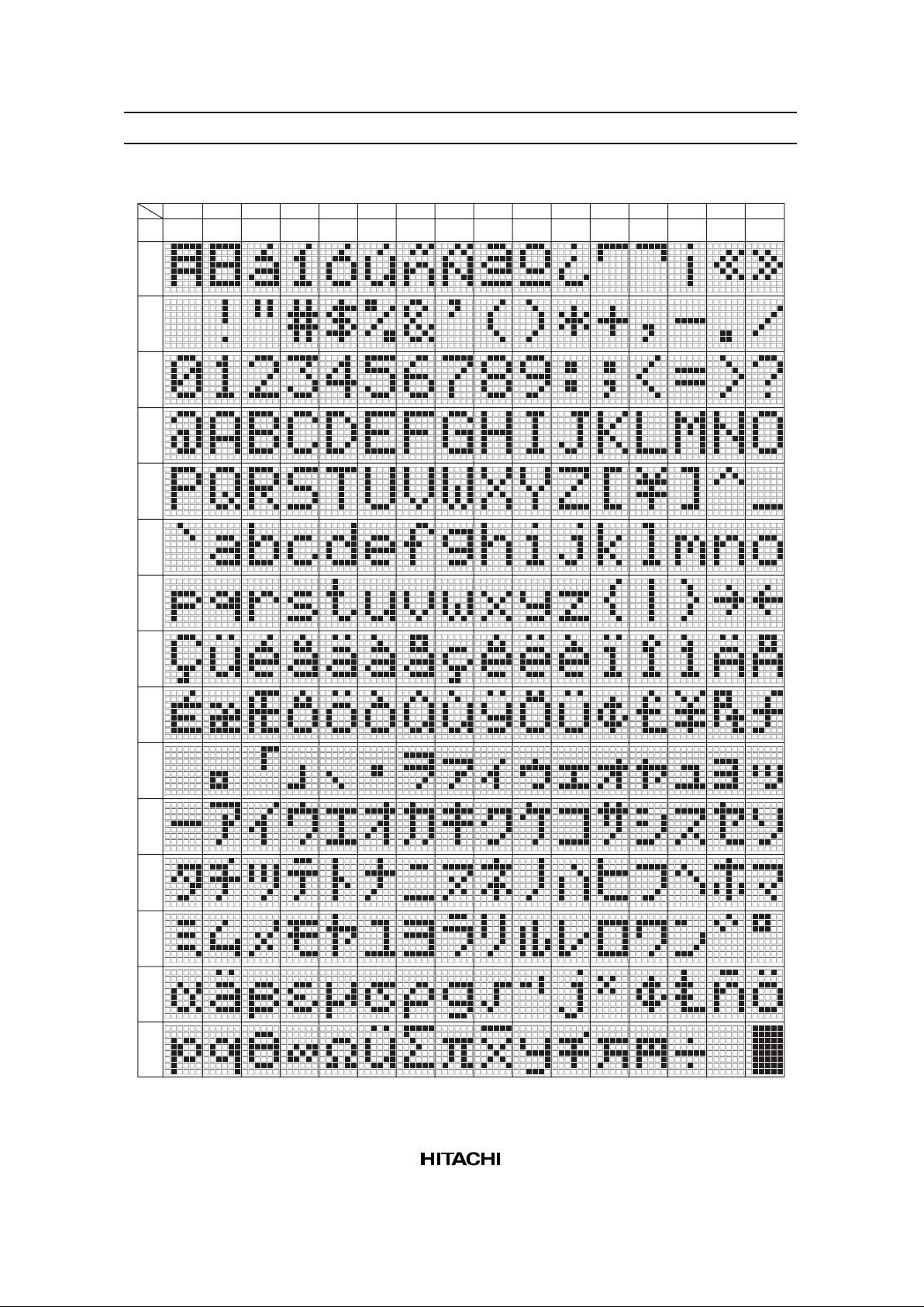
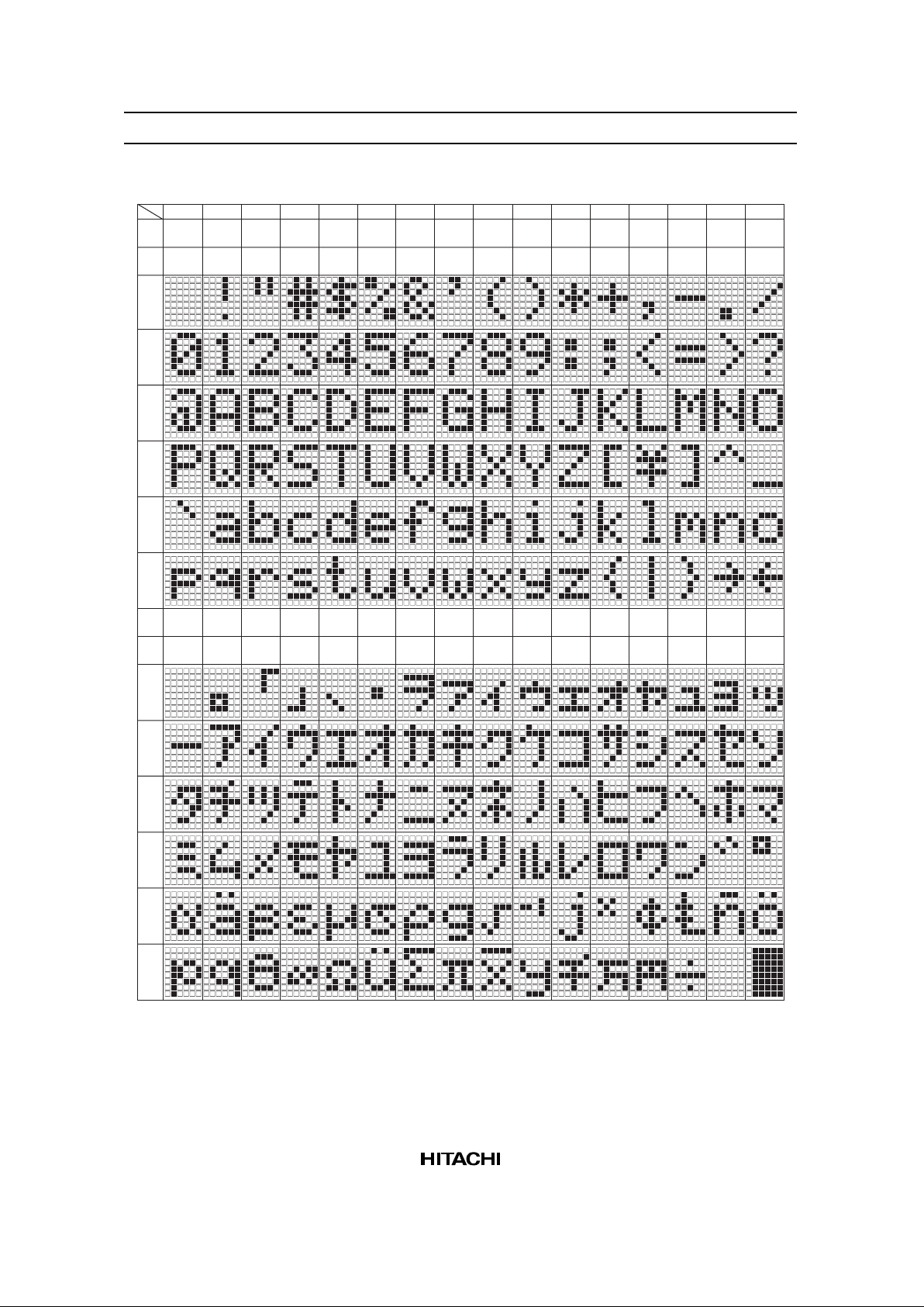
Table 6 illustrates the relation between character codes and character patterns for the Hitachi standard
CGROM. User-defined character patterns are also available using a mask-programmed ROM (see the
Modifying Character Patterns section).
Character Generator RAM (CGRAM)
The character generator RAM (CGRAM) allows the user to redefine the character patterns in the character
display mode. Up to 64 character patterns of 6 x 8-dot characters can be simultaneously displayed. The
DDRAM-specified character code can be selected to display one of these user font patterns.
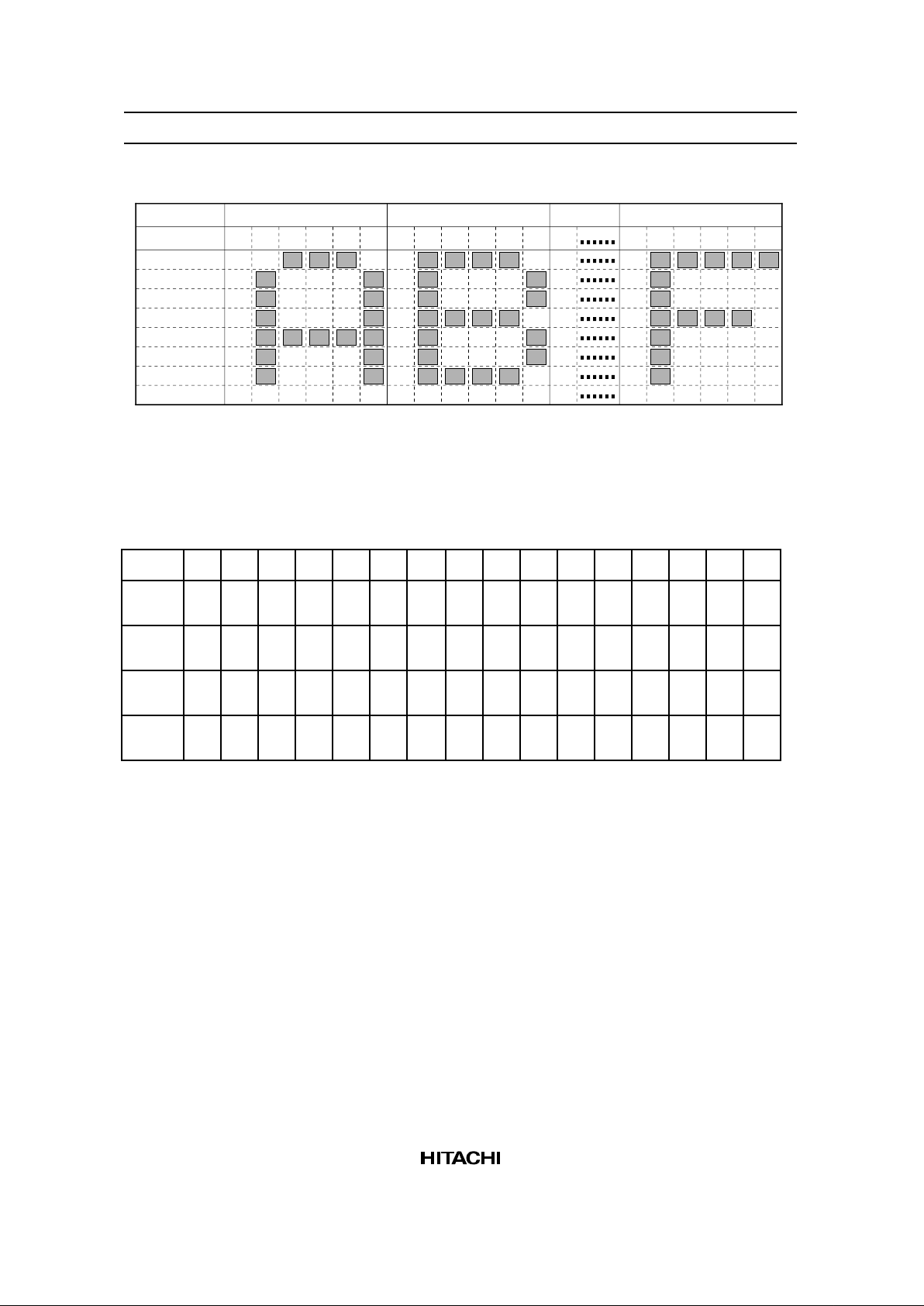
The CGRAM serves as a RAM to store 72 x 24-dot (96 x 24-dot) bit pattern data in the graphics display
mode. Here, display patterns are directly written to the CGRAM. Character codes set in the DDRAM are
not used. For details, see the Graphics Display Function section.
Segment RAM (SEGRAM)
The segment RAM (SEGRAM) is used to enable control of segments such as icons and marks through the
user program. Segments and characters are driven by a multiplexing drive method.
The SEGRAM has a capacity of 96 × 2 bits, to control the display of a maximum of 144 (192) icons and
marks. While COMS1 and COMS2 outputs are being selected, the SEGRAM is read and segments (icons
and marks) are displayed by a multiplexing drive method (72 (96) segments each during COMS1 and
COMS2 selection).
HD66724/HD66725
21
Bits in SEGRAM corresponding to segments to be displayed are directly set by the MPU, regardless of the
contents of DDRAM and CGRAM.
Timing Generator
The timing generator generates timing signals for the operation of internal circuits such as DDRAM,
CGROM, CGRAM, and SEGRAM. The RAM read timing for display and internal operation timing by
MPU access are generated separately to avoid interference with one another. This prevents flickering in
areas other than the display area when writing the data to the DDRAM, for example.
Cursor/Blink Control Circuit
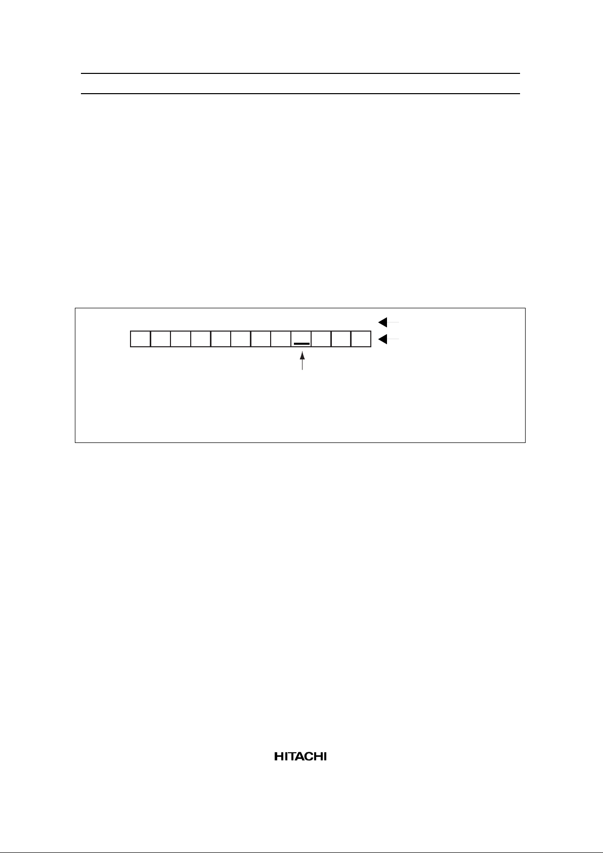
The cursor/blink (or black-white reversed) control is used to create a cursor or a flashing area on the
display in a position corresponding to the location stored in the address counter (AC).
Cursor position
Display position
DDRAM address
Note: The cursor/blink or black-white reversed control is
also active when the address counter indicates the
CGRAM or SEGRAM. However, it has no effect on the
display.
12345678 11910 12
00 01 02 03 04 05 06 07 0A08 09 0B
Figure 1 Cursor Position and DDRAM Address (When AC = 08H)
Oscillation Circuit (OSC)
The HD66724/HD66725 can provide R-C oscillation simply through the addition of an external oscillationresistor between the OSC1 and OSC2 pins. The appropriate oscillation frequency for operating voltage,
display size, and frame frequency can be obtained by adjusting the external-resistor value. Internal resistors
can be used for R-C oscillation. If this is done, care must be taken due to variations in the oscillation
frequency caused by fluctuations in internal-resistor values. Clock pulses can also be supplied externally.
Since R-C oscillation stops during the standby mode, current consumption can be reduced. For details, see
the Oscillation Circuit section.
Liquid Crystal Display Driver Circuit
The liquid crystal display driver circuit consists of 26 common signal drivers (COM1 to COM24, COMS1,
COMS2) and 72 (96) segment signal drivers (SEG1 to SEG72 (96)). When the number of lines are selected
by a program, the required common signal drivers automatically output drive waveforms, while the other
common signal drivers continue to output deselection waveforms.

HD66724/HD66725
22
The character pattern data is sent serially through a 72-bit (96-bit) shift register and latched when all
needed data has arrived. The latched data then enables the segment signal drivers to generate drive
waveform outputs.
The shift direction of 72-bit (96-bit) data can be changed by the SGS bit. The shift direction for the
common driver can also be changed by the CMS bit by selecting an appropriate direction for the device
mounting configuration.
When multiplexing drive is not used, or during the standby or sleep mode, all the above common and
segment signal drivers output the GND level, halting the display.
Booster (DC-DC Converter)
The booster doubles or triples a voltage input to the Vci pin. With this, both the internal logic units and
LCD drivers can be controlled with a single power supply. Boost output level from single to triple boost
can be software-selected. For details, see the Power Supply for Liquid Crystal Display Drive section.
V-Pin Voltage Follower
A voltage follower for each voltage level (V1 to V5) reduces current consumption by the LCD drive power
supply circuit. No external resistors are required because of the internal bleeder-resistor, which generates
different levels of LCD drive voltage. This internal bleeder-resistor can be software-specified from 1/2 bias
to 1/6.5 bias, according to the liquid crystal display drive duty value. The voltage followers can be turned
off while multiplexing drive is not being used. For details, see the Power Supply for Liquid Crystal Display
Drive section.
Contrast Adjuster
The contrast adjuster can be used to adjust LCD contrast in 32 steps by varying the LCD drive voltage by
software. This can be used to select an appropriate LCD brightness or to compensate for temperature.
Table 4 DDRAM Addresses and Display Positions
Display
Line
1st
Char.
2nd
Char.
3rd
Char.
4th
Char.
5th
Char.
6th
Char.
7th
Char.
8th
Char.
9th
Char.
10th
Char.
11th
Char.
12th
Char.
13th
Char.
14th
Char.
15th
Char.
16th
Char.
1st 00 01 02 03 04 05 06 07 08 09 0A 0B 0C 0D 0E 0F
2nd 10 11 12 13 14 15 16 17 18 19 1A 1B 1C 1D 1E 1F
3rd 20 21 22 23 24 25 26 27 28 29 2A 2B 2C 2D 2E 2F
4th 30 31 32 33 34 35 36 37 38 39 3A 3B 3C 3D 3E 3F
5th 40 41 42 43 44 45 46 47 48 49 4A 4B 4C 4D 4E 4F
Note: When SGS = 0, SEG 1/72 (96) to SEG 6/67 (91) appear at the first character at the extreme left of
the screen.
When SGS = 1, SEG 72 (96)/1 to SEG 67 (91)/6 appear at the first character at the extreme left of
the screen.

HD66724/HD66725
23
Table 5 Display-Line Modes, Display-Start Line, and DDRAM Addresses
Display-Start Lines
DisplayLine Mode
Duty
Ratio
Common
Pins
1st Line
(SN = 000)
2nd Line
(SN = 001)
3rd Line
(SN = 010)
4th Line
(SN = 011)
5th Line
(SN = 100)
1-line
(NL = 001)
1/10 COM1–
COM8
00H–0FH 10H–1FH 20H–2FH 30H–3FH 40H–4FH
2-line
(NL = 010)
1/18 COM1–
COM8
00H–0FH 10H–1FH 20H–2FH 30H–3FH 40H–4FH
2-line
(NL = 010)
1/18 COM9–
COM16
10H–1FH 20H–2FH 30H–3FH 40H–4FH 00H–0FH
3-line
(NL = 011)
1/26 COM1–
COM8
00H–0FH 10H–1FH 20H–2FH 30H–3FH 40H–4FH
3-line
(NL = 011)
1/26 COM9–
COM16
10H–1FH 20H–2FH 30H–3FH 40H–4FH 00H–0FH
3-line
(NL = 011)
1/26 COM17–
COM24
20H–2FH 30H–3FH 40H–4FH 00H–0FH 10H–1FH
HD66724/HD66725
24
Table 6 CGROM Memory Bank 0 (ROM Bit = 0)
CGRAM
(1)
CGRAM
(16)
CGRAM
(15)
CGRAM
(14)
CGRAM
(13)
CGRAM
(12)
CGRAM
(11)
CGRAM
(10)
CGRAM
(9)
CGRAM
(8)
CGRAM
(7)
CGRAM
(6)
CGRAM
(5)
CGRAM
(4)
CGRAM
(3)
CGRAM
(2)
x 0 x Fx Ex Dx Cx Bx Ax 9x 8x 7x 6x 5x 4x 3x 2x 1
1 y
2 y
3 y
4 y
5 y
6 y
7 y
8 y
9 y
A y
B y
C y
D y
E y
F y
0 y
Lower
bits
Upper
bits
HD66724/HD66725
25
Table 7 CGROM Memory Bank 1 (ROM Bit = 1)
CGRAM
(1)
CGRAM
(16)
CGRAM
(15)
CGRAM
(14)
CGRAM
(13)
CGRAM
(12)
CGRAM
(11)
CGRAM
(10)
CGRAM
(9)
CGRAM
(8)
CGRAM
(7)
CGRAM
(6)
CGRAM
(5)
CGRAM
(4)
CGRAM
(3)
CGRAM
(2)
CGRAM
(33)
CGRAM
(48)
CGRAM
(47)
CGRAM
(46)
CGRAM
(45)
CGRAM
(44)
CGRAM
(43)
CGRAM
(42)
CGRAM
(41)
CGRAM
(40)
CGRAM
(39)
CGRAM
(38)
CGRAM
(37)
CGRAM
(36)
CGRAM
(35)
CGRAM
(34)
CGRAM
(49)
CGRAM
(64)
CGRAM
(63)
CGRAM
(62)
CGRAM
(61)
CGRAM
(60)
CGRAM
(59)
CGRAM
(58)
CGRAM
(57)
CGRAM
(56)
CGRAM
(55)
CGRAM
(54)
CGRAM
(53)
CGRAM
(52)
CGRAM
(51)
CGRAM
(50)
x 0 x Fx Ex Dx Cx Bx Ax 9x 8x 7x 6x 5x 4x 3x 2x 1
2 y
3 y
4 y
5 y
6 y
7 y
8 y
9 y
A y
B y
C y
D y
E y
F y
Lower
Upper
CGRAM
(17)
CGRAM
(32)
CGRAM
(31)
CGRAM
(30)
CGRAM
(29)
CGRAM
(28)
CGRAM
(27)
CGRAM
(26)
CGRAM
(25)
CGRAM
(24)
CGRAM
(23)
CGRAM
(22)
CGRAM
(21)
CGRAM
(20)
CGRAM
(19)
CGRAM
(18)
0 y
1 y
bits
bits

HD66724/HD66725
26
CGRAM Address Map
Table 8 Relationship between Character Display Mode (GR = 0) and CGRAM Address
Font Bank Memory Bank: ROM = 0, 1
Character
Code
"00"H "01"H "02"H "03"H "04"H "05"H "06"H "07"H "08"H "09"H "0A"H "0B"H "0C"H "0D"H "0E"H "0F"H
CGRAM
Address
(HEX)
000
to
005
006
to
00B
00C
to
011
012
to
017
018
to
01D
01E
to
023
024
to
029
02A
to
02F
030
to
035
036
to
03B
03C
to
041
042
to
047
048
to
04D
04E
to
053
054
to
059
05A
to
05F
Font Bank Memory Bank: ROM = 1
Character
Code
"10"H "11"H "12"H "13"H "14"H "15"H "16"H "17"H "18"H "19"H "1A"H "1B"H "1C"H "1D"H "1E"H "1F"H
CGRAM
Address
(HEX)
100
to
105
106
to
10B
10C
to
111
112
to
117
118
to
11D
11E
to
123
124
to
129
12A
to
12F
130
to
135
136
to
13B
13C
to
141
142
to
147
148
to
14D
14E
to
153
154
to
159
15A
to
15F
Font Bank Memory Bank: ROM = 1
Character
Code
"80"H "81"H "82"H "83"H "84"H "85"H "86"H "87"H "88"H "89"H "8A"H "8B"H "8C"H "8D"H "8E"H "8F"H
CGRAM
Address
(HEX)
200
to
205
206
to
20B
20C
to
211
212
to
217
218
to
21D
21E
to
223
224
to
229
22A
to
22F
230
to
235
236
to
23B
23C
to
241
242
to
247
248
to
24D
24E
to
253
254
to
259
25A
to
25F
Font Bank Memory Bank: ROM = 1
Character
Code
"90"H "91"H "92"H "93"H "94"H "95"H "96"H "97"H "98"H "99"H "9A"H "9B"H "9C"H "9D"H "9E"H "9F"H
CGRAM
Address
(HEX)
300
to
305
306
to
30B
30C
to
311
312
to
317
318
to
31D
31E
to
323
324
to
329
32A
to
32F
330
to
335
336
to
33B
33C
to
341
342
to
347
348
to
34D
34E
to
353
354
to
359
35A
to
35F
Notes: 1. In the character display mode (GR = 0), CGRAM font pattern is displayed using character codes
set to DDRAM as per the above table. In the graphics display mode (GR
= 1), CGRAM data is
displayed irrespective of the DDRAM set data (character code).
2. When the memory bank switching bit generates ROM
= 0, CGRAM fonts for 16 character codes
"00"H to "0F"H can be displayed. When ROM
= 1, CGRAM fonts for 64 character codes "00"H to
"1F"H and "80"H to "9F"H can be displayed.
HD66724/HD66725
27
Table 9 Relationship between CGRAM Address and Character Pattern (CGRAM Data)
1111
000 001 002 003 004 005 006 007 008 009 00A 00B 00C
35A 35B 35C 35D 35E 35F
DB0
DB1
DB2
DB3
DB4
DB5
DB6
DB7
0
1
1
1
1
1
1
0
1
0
0
0
1
0
0
0
1
0
0
0
1
0
0
0
1
0
0
0
1
0
0
0
0
1
0
0
0
0
0
0
0
0
1
0
0
0
0
0
0
0
0
0
0
0
0
0
0
0
0
0
0
0
0
0
0
0
0
0
0
0
00
0
0
0
0
0
0
0
0
0
0
0
0
0
0
0
0
0
0
0
0
0
0
0
0
0
0
0
0
0
0
0
0
0
1
1
1
1
1
0
1
1
1
1
1
1
111
111
111
1
1
1
1
1
1
1
1
1
1
1
111
"00"H "01"H
"8F"H
1
0
0
0
0
0
0
0
0
Notes: 1. The least significant bit (LSB) of write data is displayed on the first line. The most significant bit (MSB) is
displayed on the 8th raster-row.
2. The 8th raster-row is the cursor position and its display is formed by a logical OR with the cursor.
3. A set bit in the CGRAM data corresponds to display selection (lit) and 0 to non-selection (unlit).
Character Code
CGRAM Address
Table 10 Relationship between Display Position and CGRAM Address in Graphics Display Mode
(GR = 1)
Display
Line
1st
Char.
2nd
Char.
3rd
Char.
4th
Char.
5th
Char.
6th
Char.
7th
Char.
8th
Char.
9th
Char.
10th
Char.
11th
Char.
12th
Char.
13th
Char.
14th
Char.
15th
Char.
16th
Char.
1st 000
to
005
006
to
00B
00C
to
011
012
to
017
018
to
01D
01E
to
023
024
to
029
02A
to
02F
030
to
035
036
to
03B
03C
to
041
042
to
047
048
to
04D
04E
to
053
054
to
059
05A
to
05F
2nd 100
to
105
106
to
10B
10C
to
111
112
to
117
118
to
11D
11E
to
123
124
to
129
12A
to
12F
130
to
135
136
to
13B
13C
to
141
142
to
147
148
to
14D
14E
to
153
154
to
159
15A
to
15F
3rd 202
to
205
206
to
20B
20C
to
211
212
to
217
218
to
21D
21E
to
223
224
to
229
22A
to
22F
230
to
235
236
to
23B
23C
to
241
242
to
247
248
to
24D
24E
to
253
254
to
259
25A
to
25F
4th 303
to
305
306
to
30B
33C
to
311
312
to
317
318
to
31D
31E
to
323
324
to
329
32A
to
32F
330
to
335
336
to
33B
33C
to
341
342
to
347
348
to
34D
34E
to
353
354
to
359
35A
to
35F
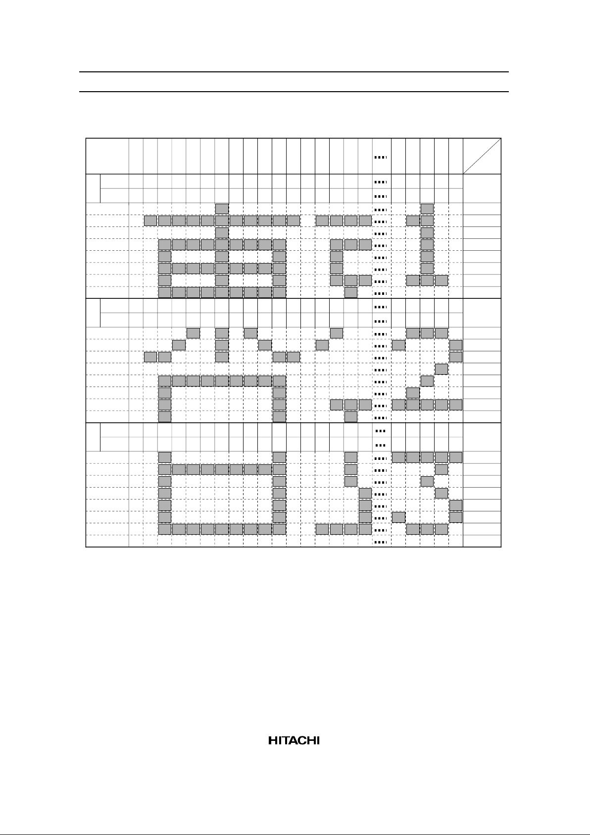
Notes: 1. In the graphic display mode (GR = 1), graphics pattern is displayed using bitmap data set to
CGRAM as per the above table.
2. Each display character and display line are converted to 6-dot width/character and 8 dots/line,
respectively.
3. The 4th line is displayed by vertical smooth scroll operation.
HD66724/HD66725
28
Table 11 Relationship between CGRAM Address and Screen Display Position in Graphics
Display Mode (GR = 1) (HD66724)
DB0
000
DB1
DB2
DB3
DB4
DB5
DB6
DB7
001 002 003 004 005 006 007 008 009 00A 00B
00C
00D 00E 00F 010
046 047
045044043
COM1
COM2
COM3
COM4
COM5
COM6
COM7
COM8
DB0
100
DB1
DB2
DB3
DB4
DB5
DB6
DB7
101 102 103 104 105 106 107 108 109 10A 10B 10C 10D 10E 10F 110
146 147145144143
COM9
COM10
COM11
COM12
COM13
COM14
COM15
COM16
DB0
200
DB1
DB2
DB3
DB4
DB5
DB6
DB7
201 202 203 204 205 206 207 208 209 20A 20B 20C 20D
20E 20F 210
246 247245244243
COM17
COM18
COM19
COM20
COM21
COM22
COM23
COM24
SEG1/72
SEG2/71
SEG3/70
SEG4/69
SEG5/68
SEG6/67
SEG7/66
SEG8/65
SEG9/64
SEG10/63
SEG11/62
SEG12/61
SEG13/60
SEG14/59
SEG15/58
SEG16/57
SEG17/56
SEG68/5
SEG69/4
SEG70/3
SEG71/2
SEG72/1
1
1
1
1
1
1
1
1
11111 1 1 1 1 1
1111 1 1 1 1
1111 1 1 1 1
1111 1 1 1 1
1 1
1 1
1
1
1
1
1
11
1
1
1 1
1 1 1 1
1 1 1
1 1 1
1
1
1
1
1
1
1
1
1
1
1
11 1
1
11
1
1
1
1
1
1
1
1 1 1 1 1
1 1 1 1 1
1
1
1
1
1
111
1
1 1 1 1 1 1 1 1 1
1 1
1 1
1 1
1 1
1 1
1 1
1 1
1 1
1 1 1 1 1 1 1 1 1
1 1 1 1 1 1 1 1 1
1 1 1
11 1 1
1
1
1
1
1
1
1
00000
00000
0
0
0
0
0
000000000
0
0
0
00000000000000000000000
0
0
00
00
00
000000
0
0
0
0
0
0
0
0
0
0
0
0
0
0
000
000
000
000
0000
00
00
0
00
00
00
00
00
00
0
0
0
0
0
0
0
0
0
0
0
0
00
000
0
0
0
000
000
000
000
000
0
0
0
0
0
0
0
0
0
0
0
0
0
0
0
0
0
0
0
0
0
0
0
0
0
0
0
0
0
0
0
0
0
0
0
0
0
0
0
0
0
0
0
0
0
0
0
0
0
0
0
0
0
0
0
0
0
0
0
00000000000
000000
0000
00
0000
000000
0
00
0
0
0
0
0
0000000000000000 00000
000
000
0000
00
00
000000
00
00000
0 000
0000
00
00
0
0
000
0
0
00
00
00
00
00
00
00
00
00
00
00
00
(HEX)
(HEX)
(HEX)
0
0
0
0
0
0
0
0
0
0
0
0
0
0
0
0
0
0
0
0
0
0
0
0
047 046 045 044 043 042 041 040 03F 02E03D03C
03B 03A 039 038 037 001 000002003004
SGS="0"
SGS="1"
SGS="0"
SGS="1"
147 146 145 144 143 142 141 140 13F 13E 13D13C 13B 13A 139 138 137 101 100102103104
SGS="0"
SGS="1"
247 246 245 244 243 242 241 240 23F 23E23D23C 23B 23A 239 238 237 201 200203204205
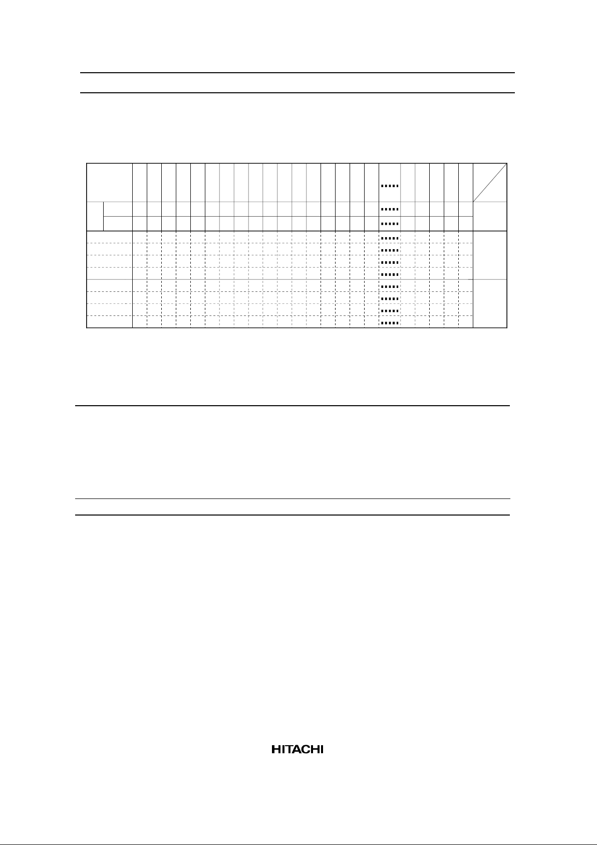
Notes: 1. In the graphics display mode (GR=1), the CGRAM data is displayed irrespective of the DDRAM set data.
2. The HD66725 can display addresses from 000H to 35FH.
3. A set bit in the CGRAM data corresponds to display selection (lit) and 0 to non-selection (unlit).
Segment
Driver
Segment
Common
Address
AddressAddress
HD66724/HD66725
29
SEGRAM Address Map
Table 12 Relationship between SEGRAM Address and Screen Display Position (HD66724)
DB0
00
DB1
DB2
DB7
01 02 03 04 05 06 07 08 09 0A 0B 0C 0D 0E 0F 10 46 47454443
COMS1
COMS2
SEG1/72
SEG2/71
SEG3/70
SEG4/69
SEG5/68
SEG6/67
SEG7/66
SEG8/65
SEG9/64
SEG10/63
SEG11/62
SEG12/61
SEG13/60
SEG14/59
SEG15/58
SEG16/57
SEG17/56
SEG68/5
SEG69/4
SEG70/3
SEG71/2
SEG72/1
0/1
0/1
0/1
0/1
0/1
0/1
0/1
0/1
0/1
0/1
0/1
0/1
0/1
0/1
0/1
0/1
0/1
0/1
0/1
0/1
0/1
0/1
0/1
0/1
0/1
0/1
0/1
0/1
0/1
0/1
0/1
0/1
0/1
0/1
0/1
0/1
0/1
0/1
0/1
0/1
0/1
0/1
0/1
0/1
(HEX)
DB3
DB4
DB5
DB6
0/10/10/10/10/10/10/10/10/10/10/10/10/10/10/10/10/1
0/10/10/10/10/10/10/10/10/10/10/10/10/10/10/10/10/1
0/10/10/10/10/10/10/10/10/10/10/10/10/10/10/10/10/1
0/10/10/10/10/10/10/10/10/10/10/10/10/10/10/10/10/1
0/10/10/10/10/10/10/10/10/10/10/10/10/10/10/10/10/1
0/10/10/10/10/10/10/10/10/10/10/10/10/10/10/10/10/1
0/10/10/10/10/1
0/10/10/10/10/1
0/10/10/10/10/1
0/10/10/10/10/1
0/10/10/10/10/1
0/10/10/10/10/1
47 46 45 44 43 42 41 40 3F 3E 3D 3C 3B 3A 39 38 37
01 00020304
SGS=0
Segment
Driver
SGS=1
Segment
Common
Address
Note: The HD66725 can display addresses from 00H to 5FH.
Table 13 Relationship between Segment Driver Output Pin and Segment Display Function
(HD66724)
When SGS = 0 When SGS = 1 Segment Output Control
SEG1/72, SEG4/69, SEG7/66,
SEG10/63, SEG13/60, SEG16/57,
SEG19/54, SEG22/51, SEG25/48,
SEG28/45, SEG31/42, SEG34/39,
SEG37/36, SEG40/33, SEG43/30,
SEG46/27, SEG49/24, SEG52/21,
SEG55/18, SEG58/15, SEG61/12,
SEG64/9, SEG67/6, SEG70/3
SEG72/1, SEG69/4, SEG66/7,
SEG63/10, SEG60/13, SEG57/16,
SEG54/19, SEG51/22, SEG48/25,
SEG45/28, SEG42/31, SEG39/34,
SEG36/37, SEG33/40, SEG30/43,
SEG27/46, SEG24/49, SEG21/52,
SEG18/55, SEG15/58, SEG12/61,
SEG9/64, SEG6/67, SEG3/70
Grayscale segment display allowed
(Reflective color segment supported)
Output pins other than above Output pins other than above Segment blinking allowed

HD66724/HD66725
30
Table 14 Relationship between Segment Driver Output Pin and Segment Display Function
(HD66725)
When SGS = 0 When SGS = 1 Segment Output Control
SEG1/96, SEG4/93, SEG7/90,
SEG10/87, SEG13/84, SEG16/81,
SEG19/78, SEG22/75, SEG25/72,
SEG28/69, SEG31/66, SEG34/63,
SEG37/60, SEG40/57, SEG43/54,
SEG46/51, SEG49/48, SEG52/45,
SEG55/42, SEG58/39, SEG61/36,
SEG64/33, SEG67/30, SEG70/27,
SEG73/24, SEG74/21, SEG79/18,
SEG82/15, SEG85/12, SEG88/9,
SEG91/6, SEG94/3
SEG96/1, SEG93/4, SEG90/7,
SEG87/10, SEG84/13, SEG81/16,
SEG78/19, SEG75/22, SEG72/25,
SEG69/28, SEG66/31, SEG63/34,
SEG60/37, SEG57/40, SEG54/43,
SEG51/46, SEG48/49, SEG45/52,
SEG42/55, SEG39/58, SEG36/61,
SEG33/64, SEG30/67, SEG27/70,
SEG24/73, SEG21/76, SEG18/79,
SEG15/82, SEG12/85, SEG9/88,
SEG6/91, SEG3/94
Grayscale segment display allowed
(Reflective color segment supported)
Output pins other than above Output pins other than above Segment blinking allowed
Note: For details, see the Reflective Color Mark/Blink Mark Display section.
Table 15 Relationship between SEGRAM Data and Grayscale Control Segment Display
SEGRAM Data
Setting
Effective Applied Voltage
SEGRAM Data
Setting
Effective Applied Voltage
DB3 DB2 DB1 DB0 for COMS1 Segment DB7 DB6 DB5 DB4 for COMS2 Segment
0 0 0 0 0 (Always unlit) 0 0 0 0 0 (Always unlit)
0 0 0 1 1 (Always lit) 0 0 0 1 1 (Always lit)
0 0 1 0 0.34 (Grayscale display) 0 0 1 0 0.34 (Grayscale display)
0 0 1 1 0.38 (Grayscale display) 0 0 1 1 0.38 (Grayscale display)
0 1 0 0 0.41 (Grayscale display) 0 1 0 0 0.41 (Grayscale display)
0 1 0 1 0.44 (Grayscale display) 0 1 0 1 0.44 (Grayscale display)
0 1 1 0 0.47 (Grayscale display) 0 1 1 0 0.47 (Grayscale display)
0 1 1 1 0.50 (Grayscale display) 0 1 1 1 0.50 (Grayscale display)
1 0 0 0 (Blink display) *
1
1 0 0 0 (Blink display) *
1
1 0 0 1 0.53 (Grayscale display) 1 0 0 1 0.53 (Grayscale display)
1 0 1 0 0.56 (Grayscale display) 1 0 1 0 0.56 (Grayscale display)
1 0 1 1 0.59 (Grayscale display) 1 0 1 1 0.59 (Grayscale display)
1 1 0 0 0.63 (Grayscale display) 1 1 0 0 0.63 (Grayscale display)
1 1 0 1 0.66 (Grayscale display) 1 1 0 1 0.66 (Grayscale display)
1 1 1 0 0.69 (Grayscale display) 1 1 1 0 0.69 (Grayscale display)
1 1 1 1 0.72 (Grayscale display) 1 1 1 1 0.72 (Grayscale display)
Note: Blinking is provided by repeatedly turning on the segment for 32 frames and turning it off for the next
32 frames.
 Loading...