

HAT1043M
Silicon P Channel Power MOS FET
Power Switching
Features
• Low on-resistance
• Low drive current
• High density mounting
• 2.5 V gate drive device can be driven from 3 V source
Outline
ADE-208-754D (Z)
5th Edition
February 1999
TSOP–6
3
G
12 5 6
DSD
DD
4
4
5
6
1
4 Source
3 Gate
1, 2, 5, 6 Drain
3
2

HAT1043M
Absolute Maximum Ratings (Ta = 25°C)
Item Symbol Ratings Unit
Drain to source voltage V
Gate to source voltage V
Drain current I
Drain peak current I
Body-drain diode reverse drain current I
Channel dissipation Pch
DSS
GSS
D
D(pulse)
DR
Pch
Note 2
(pulse)
(continuous)
Note 1
Note 2
Note 3
Channel temperature Tch 150 °C
Storage temperature Tstg –55 to +150 °C
Note: 1. PW ≤ 10 µs, duty cycle ≤ 1%
2. When using the alumina ceramic board (50 x 50 x 0.7 mm), PW ≤ 5 s, Ta = 25°C
3. When using the alumina ceramic board (50 x 50 x 0.7 mm), Ta = 25°C
Electrical Characteristics (Ta = 25°C)
Item Symbol Min Typ Max Unit Test Conditions
Drain to source breakdown voltage V
Gate to source leak current I
Zero gate voltege drain current I
Gate to source cutoff voltage V
Static drain to source on state R
(BR)DSS
GSS
DSS
GS(off)
DS(on)
resistance — 85 110 mΩ ID = –3 A, VGS = –2.5 V
Forward transfer admittance |yfs|47—SI
Input capacitance Ciss — 750 — pF VDS = –10 V
Output capacitance Coss — 310 — pF VGS = 0
Reverse transfer capacitance Crss — 220 — pF f = 1 MHz
Total Gate charge Qg — 11 — nc VDD = –10 V
Gate to Source charge Qgs — 2 — nc VGS = –4.5 V
Gate to Drain charge Qgd — 3.5 — nc ID= –4.4 A
Turn-on delay time t
Rise time t
Turn-off delay time t
Fall time t
Body–drain diode forward voltage V
Body–drain diode reverse
t
d(on)
r
d(off)
f
DF
rr
recovery time
Note: 1. Pulse test
–20 — — V ID = –10 mA, VGS = 0
——±0.1 µAVGS = ±12 V, VDS = 0
——–1µAVDS = –20 V, VGS = 0
–0.4 — –1.4 V ID = –1 mA, VDS = –10 V
—5565mΩ ID = –3 A, VGS = –4.5 V
— 15 — ns VGS = –4.5 V, ID = –3 A
— 100 — ns RL = 3.3 Ω
—85—ns
— 100 — ns
— –0.95 –1.23 V IF = –4.4 A, VGS = 0
— 50 — ns IF = –4.4 A, VGS = 0
–20 V
±12 V
–4.4 A
–17.6 A
–4.4 A
2.0 W
1.05 W
= –3 A, VDS = –10 V
D
diF/ dt = –20 A/ µs
Note 1
Note 1
Note 1
2
Main Characteristics
HAT1043M
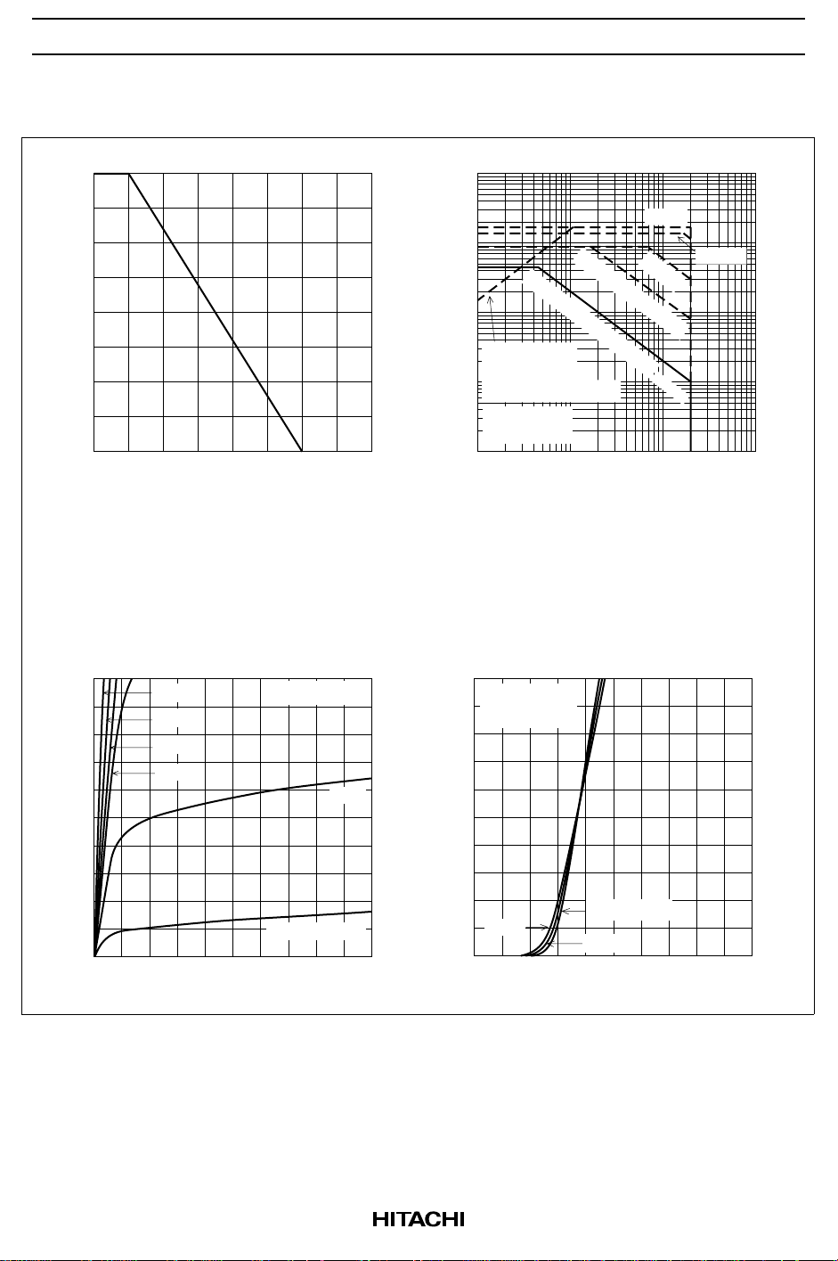
Power vs. Temperature Derating
2.0
1.5
1.0
0.5
Channel Dissipation Pch (W)
0
50 100 150 200
Ambient Temperature Ta (°C)
Test Condition
When using the alumina ceramic board
(50x50x0.7mm),(PW ≤ 5s)
Typical Output Characteristics
-10
-10 V
-4 V
-8
D
-3 V
-2.5 V
-6
Pulse Test
-2 V
-100
Maximum Safe Operation Area
-30
-10
D
-3
PW = 10 ms (1 shot)
DC Operation (PW ≤ 5s)
10 µs
1 ms
100 µs
-1
-0.3
Operation in
-0.1
-0.03
-0.01
this area is
limited by R
Ta = 25°C
1 shot pulse
DS(on)
Drain Current I (A)
-0.1 -0.3 -1
Drain to Source Voltage V (V)
-3
Note1
-10
-30
DS
Note 1 When using the alumina ceramic board
( 50x50x0.7mm)
Typical Transfer Characteristics
-10
V = -10 V
DS
Pulse Test
-8
D
-6
-100
-4
Drain Current I (A)
-2
0
-2 -4 -6 -8 -10
Drain to Source Voltage V (V)
V = -1.5 V
GS
DS
-4
Drain Current I (A)
-2
Tc = –25°C
75°C
25°C
0
-1 -2 -3 -4 -5
Gate to Source Voltage V (V)
GS
3
 Loading...