HIT HAF2007-S, HAF2007-L Datasheet

HAF2007(L), HAF2007(S)
Silicon N Channel MOS FET Series
Power Switching
Target specification
ADE-208-706 (Z)
1st. Edition
Dec. 1998
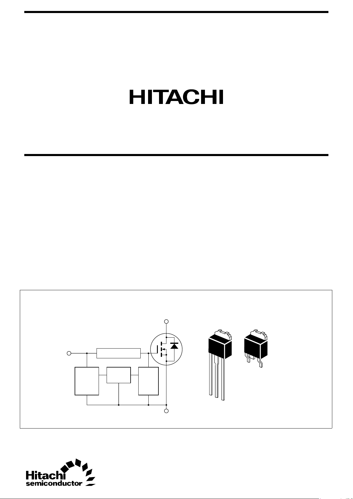
This FET has the over temperature shut–down capability sensing to the junction temperature. This FET has
the built–in over temperature shut–down circuit in the gate area. And this circuit operation to shut–down
the gate voltage in case of high junction temperature like applying over power consumption, over current
etc.
Features
• Logic level operation (4 to 6 V Gate drive)
• High endurance capability against to the short circuit
• Built–in the over temperature shut–down circuit
• Latch type shut–down operation (Need 0 voltage recovery)
Outline
1
2
3
4
4
1
2
3
1. Gate
2. Drain
3. Source
4. Drain
DPAK–2
Gate resistor
Tempe–
rature
Sencing
Circuit
Latch
Circuit
Gate
Shut–
down
Circuit
D
S
G
2, 4
1
3

HAF2007(L), HAF2007(S)
2
Absolute Maximum Ratings (Ta = 25°C)
Item Symbol Ratings Unit
Drain to source voltage V
DSS
60 V
Gate to source voltage V
GSS
(16) V
Gate to source voltage V
GSS
(–2.5) V
Drain current I
D
5A
Drain peak current I
D(pulse)
Note1
10 A
Body-drain diode reverse drain current I
DR
5A
Channel dissipation Pch
Note2
20 W
Channel temperature Tch 150 °C
Storage temperature Tstg –55 to +150 °C
Note: 1. PW ≤ 10µs, duty cycle ≤ 1 %
2. Value at Ta = 25°C
Typical Operation Characteristics
Item Symbol Min Typ Max Unit Test Conditions
Input voltage V
IH
3.5 — — V
V
IL
— — 1.2 V
Input current I
IH1
— — 100 µA Vi = 8V, VDS = 0
(Gate non shut down) I
IH2
——50µA Vi = 3.5V, VDS = 0
I
IL
——1 µA Vi = 1.2V, VDS = 0
Input current I
IH(sd)1
— 0.8 — mA Vi = 8V, VDS = 0
(Gate non shut down) I
IH(sd)2
— 0.35 — mA Vi = 3.5V, VDS = 0
Shut down temperature T
sd
— 175 — °C Channel temperature
Gate operation voltage V
op
3.5 — 12 V
 Loading...