HIT HAF1001 Datasheet

HAF1001
Silicon P Channel MOS FET Series
Power Switching / Over Temperature Shut–down Capability
ADE-208-583 A (Z)
2nd Edition
October 1997
Features
This FET has the over temperature shut–down capability sensing to the junction temperature.
This FET has the built–in over temperature shut–down circuit in the gate area. And this circuit
operation to shut–down the gate voltage in case of high junction temperature like applying over power
consumption, over current etc.
• Logic level operation (–4 to –6 V Gate drive)
• High endurance capability against to the short circuit
• Built–in the over temperature shut–down circuit
• Latch type shut–down operation (Need 0 voltage recovery)
Outline
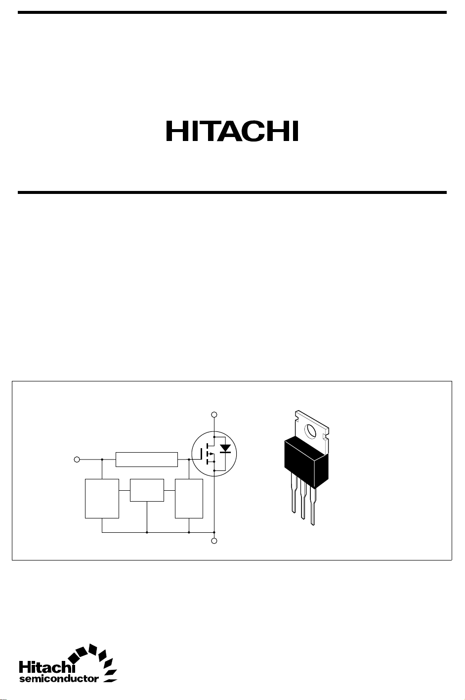
TO–220AB
G
Tempe–
rature
Sencing
Circuit
Gate resistor
Latch
Circuit
Gate
Shut–
down
Circuit
D
S
4
1
2
3
1. Gate
2. Drain
3. Source
4. Drain

HAF1001
Absolute Maximum Ratings (Ta = 25°C)
Item Symbol Ratings Unit
Drain to source voltage V
Gate to source voltage V
Gate to source voltage V
Drain current I
Drain peak current I
Body-drain diode reverse drain current I
Channel dissipation Pch
DSS
GSS+
GSS–
D
D(pulse)
DR
Note1
Note2
Channel temperature Tch 150 °C
Storage temperature Tstg –55 to +150 °C
Note: 1. PW ≤ 10µs, duty cycle ≤ 1 %
2. Value at Tc = 25°C
Typical Operation Characteristics
Item Symbol Min Typ Max Unit Test Conditions
Input voltage V
Input current I
(Gate non shut down) I
Input current I
(Gate shut down) I
Shut down temperature T
Gate operation voltage V
V
IH1
IH2
I
IL
IH(sd)1
IH(sd)2
sd
IH
IL
OP
–3.5 — — V
— — –1.2 V
— — –100 µA Vi = –8V, VDS = 0
— — –50 µA Vi = –3.5V, VDS = 0
——–1µA Vi = –1.2V, VDS = 0
— –0.8 — mA Vi = –8V, VDS = 0
— –0.35 — mA Vi = –3.5V, VDS = 0
— 175 — °C Channel temperature
–3.5 — –13 V
–60 V
–16 V
3V
–15 A
–30 A
–15 A
50 W
2

HAF1001
Electrical Characteristics (Ta = 25°C)
Item Symbol Min Typ Max Unit Test Conditions
Drain current I
Drain current I
Drain to source breakdown
D1
D2
V
(BR)DSS
voltage
Gate to source breakdown
V
(BR)GSS+
voltage
Gate to source breakdown
V
(BR)GSS–
voltage
Gate to source leak current I
Input current (shut down) I
Zero gate voltege drain current I
Gate to source cutoff voltage V
Static drain to source on state
GSS+1
I
GSS+2
I
GSS+3
I
GSS–
GS(op)1
I
GS(op)1
DSS
GS(off)
R
DS(on)
resistance
Static drain to source on state
R
DS(on)
resistance
Forward transfer admittance |yfs|5 10—S I
Output capacitance Coss — 610 — pF VDS = –10V , VGS = 0
Turn-on delay time t
Rise time t
Turn-off delay time t
Fall time t
Body–drain diode forward
V
d(on)
r
d(off)
f
DF
voltage
Body–drain diode reverse
t
rr
recovery time
Over load shut down t
operation time
Note4
os1
t
os2
Note: 3. Pulse test
4. Including the junction temperature rise of the over loaded condition.
–7 — — A VGS = –3.5V, VDS = –2V
— — –10 mA VGS = –1.2V, VDS = –2V
–60 — — V ID = –10mA, VGS = 0
–16 — — V IG = –100µA, VDS = 0
3——VI
— — –100 µAV
— — –50 µAV
——–1µAV
— — 100 µAV
= 100µA, VDS = 0
G
= –8V, VDS = 0
GS
= –3.5V, VDS = 0
GS
= –1.2V, VDS = 0
GS
= 2.4V, VDS = 0
GS
— –0.8 — mA VGS = –8V, VDS = 0
— –0.35 — mA VGS = –3.5V, VDS = 0
— — –250 µAV
= –50 V, VGS = 0
DS
–1.1 — –2.25 V ID = –1mA, VDS = –10V
— 100 130 mΩ ID = –7.5A, VGS = –4V
—7090mΩ ID = –7.5A
= –10V
V
GS
= –7.5A, VDS = –10V
D
Note3
f = 1 MHz
— 7.5 — µsI
—36—µsR
= –7.5A, VGS = –5V
D
= 4Ω
L
—32—µs
—29—µs
— –1.0 — V IF = –15A, VGS = 0
— 200 — ns IF = –15A, VGS = 0
diF/ dt =50A/µs
— 3.7 — ms VGS = –5V, VDD = –12V
—1 —msV
= –5V, VDD = –24V
GS
Note3
Note3
3
 Loading...