

HA22032T
GaAs MMIC
Down Converter for Micro Wave Application
Features
• Suitable for down converter of Micro Wave Application(1.5 GHz)
• Low voltage and low current operation (3V, 9 mA typ.)
• Low noise (2 dB typ. @1.5 Ghz)
• High power gain (26 dB typ. @1.5 GHz)
• Built–in matching circuits (50 Ω)
• Small surface mount package (TSSOP-8)
ADE-207-259 (Z)
1st. Edition
May 1998
Outline
TTP-8D
This document may, wholly or partially, be subject to change without notice.
This Device si sensitive to Electro Static Discharge.
An Adequate handling procedure is requested.
HA22032
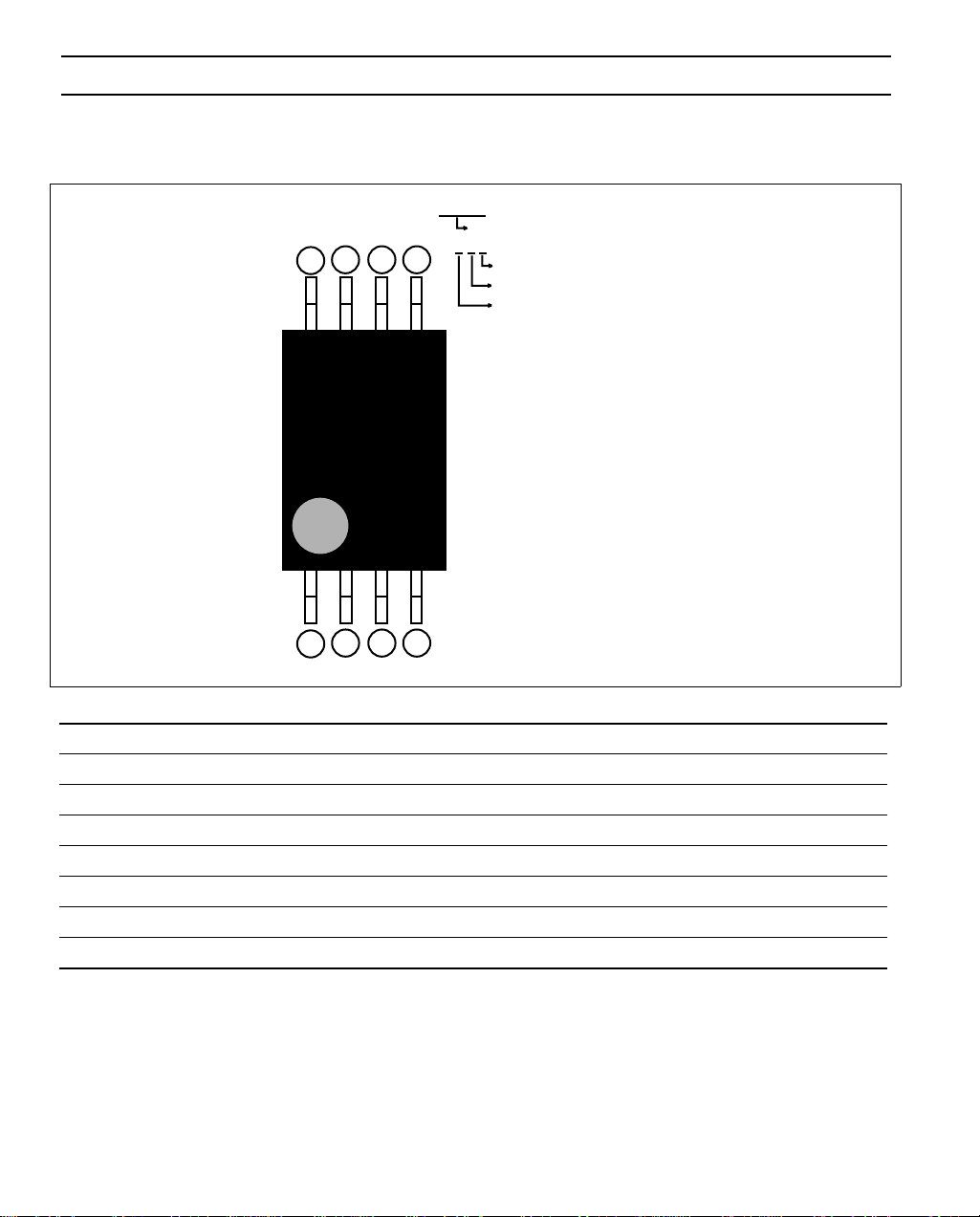
Pin Arrangement
7 6 5
8
HA32
8A1
HA32
Mark type
8A1
Weekly code(variable)
Monthly code(variable)
Yearly code(variable)
2 3 4
1
Top View
Pin No. Pin name Function
1 Vddlo Power supply (Lo)
2 Vddln Power supply (LNA)
3 GND Ground
4 RF in RF input
5 Cs Bypath capacitor (>100 pF)
6 IF out IF output
7 GND Ground
8 Lo in Local input
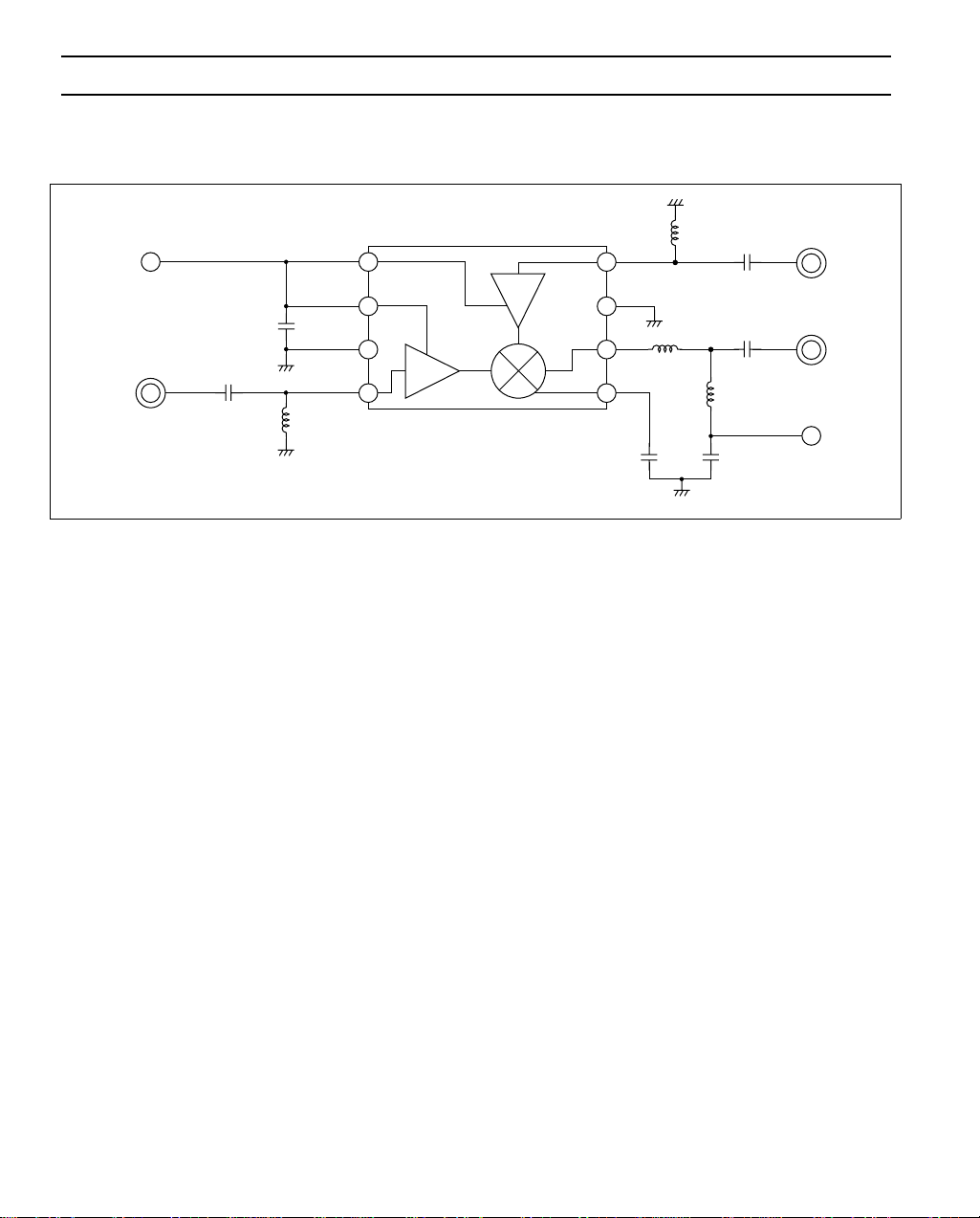
Block Diagram
HA22032
Vdd
RF in
1.5pF
*
6.8nH
2.7nH
1
2
3
4
*:1000+15pF
8
7
6
390nH
5
*
1.5pF
5pF
220nH
*
Lo in
IF out
Vdd

HA22032
Absolute Maximum Ratings (Ta = 25°C)
Item Symbol Ratings Unit
Supply voltage Vdd 5 V
Maximum current Idd 15 mA
Power dissipation Pd 100 mW
Channel temperature Tch 150 °C
Storage temperature Tstg –55 to +125 °C
Operation temperature Topr –20 to +70 °C
Maximum input power Pin max +18 dBm
Electrical Characteristics (Ta = 25°C, Vdd = 3V)
Item Symbol Min Typ Max Unit Test Conditions
Quiescent current Idd 5 9 12 mA No signal
Power gain PG 23 26 29 dB f = 1489 Mhz, fLo = 1619 Mhz,
Plo = –15 dBm, IF = 130 Mhz,
Pin = –30dBm
Noise figure NF — 2 3 dB f = 1489 Mhz, fLo = 1619 Mhz,
Plo = –15 dBm, IF = 130 MHz
Typical Performance (Ta = 25°C, Vdd = 3V)
Item Symbol Typ Unit Test Conditions
VSWR (input) VSWRin2 — f = 1.489 GHz
3rd order inter-cept point IP3o +4 dBm f = 1.489 GHz, fud =1.490 Ghz, Pin = –30 dBm,
fLo = 1.619 Ghz, Plo = –15 dBm

Main Characteristics
HA22032
Conversion gain,Noise figure
29
Vdd = 3V
Pin = –30dBm
IF = 130MHz
28
PLo = –15dBm
Ta = +25°C
27
26
25
24
vs.Frequency
CG
NF
Conversion gain CG (dB)
23
1400
1450
Frequency f (MHz)
3rd order inter-cept point(out)
3
2.5
2
8
Vdd = 3V
Pin = –30dBm
IF = 130MHz
PLo = –15dBm
Ta = +25°C
6
2 signals input
4
2
vs. Frequency
Noise figure NF (dB)
1.5
160015501500
0
3rd order inter-cept point IP3o (dBm)
1400
1450
160015501500
Frequency f (MHz)
2.5
2
VSWR
1.5
1
1475
1605
VSWR vs. Frequency
Vdd = 3V
Ta = +25°C
RF
Lo
1480
14901485
1495
Frequency(RF) RF (MHz)
1610
16201615
1625
1500
1630
1505
1635
Conversion gain,3rd order inter-cept point
29
28
27
26
25
24
Conversion gain CG (dB)
23
-55
vs. Input power
-55
-45
CG
-40
IP3o
Vdd = 3V
f = 1489MHz
fLo = 1619MHz
PLo = –15dBm
Ta = +25°C
2 signals input
-30
-35
-35
-20
Frequency f (MHz)
6
5
4
3
2
1
0
3rd order inter-cept point IP3o (dBm)

HA22032
Conversion gain,Noise figure
29
f = 1489 MHz
Pin = –30 dBm
IF = 130 MHz
28
PLo = –15 dBm
Ta = +25°C
27
26
25
24
Conversion gain CG (dB)
23
2
vs. Supply voltage
2.5
3.53
CG
NF
Supply voltage Vdd (V)
3rd order inter-cept point
vs. Supply voltage
2.5
3
2
8
f = 1489 MHz
Pin = –30 dBm
IF = 130 MHz
PLo = –15dBm
6
Ta = +25°C
2 signals input
4
2
Noise figure NF (dB)
1.5
4
4.5
5
0
3rd order inter-cept point IP3o (dBm)
2
2.5
3.53
4
4.5
5
Supply voltage Vdd (V)
2.5
RF = 1489 MHz
Lo = 1619 MHz
Ta = +25°C
2
VSWR
1.5
1
2
VSWR vs. Supply voltage
RF
Lo
2.5
3.53
4
Supply voltage Vdd (V)
4.5
Quiescent current vs. Supply voltage
12
Ta = +25°C
11
10
9
8
7
6
Quiescent current Idd (mA)
5
2
5
2.5
3.53
4
4.5
5
Supply voltage Vdd (V)

HA22032
Conversion gain,Noise figure
29
28
27
26
25
24
Conversion gain CG (dB)
23
-25
vs. Ambient temperature
CG
NF
250
Ambient Temperture Ta (°C)
Vdd = 3 V
f = 1489 MHz
Pin = –30 dBm
IF = 130 MHz
PLo = –15 dBm
50
75
3
2.5
2
8
6
4
2
Noise figure NF (dB)
1.5
0
3rd order inter-cept point IP3o (dBm)
-25
3rd order inter-cept point
vs. Ambient temperature
Vdd = 3 V
f = 1489 MHz
Pin = –30 dBm
IF = 130 MHz
PLo = –15 dBm
2 signals input
250
50
Ambient Temperature Ta (°C)
75
VSWR vs. Ambient temperature
2.5
Vdd = 3V
RF = 1489 MHz
Lo = 1619 MHz
RF
2
VSWR
1.5
1
-25
250
Ambient temperature Ta (°C)
Lo
50
75
Quiescent vs. Ambient temperature
12
Vdd = 3V
11
10
9
8
7
6
Quiescent current Idd (mA)
5
-25
250
Ambient temperature Ta (°C)
50
75

HA22032
Conversion gain,Noise figure
29
Vdd = 3V
f = 1489 MHz
Pin = –30 dBm
28
IF = 130 MHz
Ta = +25°C
27
26
25
24
Conversion gain CG (dB)
23
-50
vs. Local power
-20-25
-15
Local power PLo (dBm)
CG
NF
-10
-5
3
2.5
2
10
5
0
Noise figure NF (dB)
1.5
3rd inter-cept point IP3o (dBm)
-5
-50
3rd order inter-cept point
vs. Local power
Vdd = 3 V
f = 1489 MHz
Pin = –30 dBm
IF = 130 MHz
Ta = +25°C
2 signals input
-20-25
Local power PLo (dBm)
-15
-10
-5

Package Dimentions
3.00
3.30 Max
85
14
+0.08
0.22
0.20 ± 0.06
–0.07
4.40
0.65
M
0.13
0.805 Max*
HA22032
Unit: mm
1.0
6.40 ± 0.20
0.10
1.10 Max
Dimension including the plating thickness
Base material dimension
+0.03
–0.04
0.07
0.17 ± 0.05
0.15 ± 0.04
0° – 8°
0.50 ± 0.10
Note: Include Mold Flash
Hitachi Code
JEDEC
EIAJ
Weight
(reference value)
TTP-8D
—
—
—

HA22032
Cautions
1. Hitachi neither warrants nor grants licenses of any rights of Hitachi’s or any third party’s patent,
copyright, trademark, or other intellectual property rights for information contained in this document.
Hitachi bears no responsibility for problems that may arise with third party’s rights, including
intellectual property rights, in connection with use of the information contained in this document.
2. Products and product specifications may be subject to change without notice. Confirm that you have
received the latest product standards or specifications before final design, purchase or use.
3. Hitachi makes every attempt to ensure that its products are of high quality and reliability. However,
contact Hitachi’s sales office before using the product in an application that demands especially high
quality and reliability or where its failure or malfunction may directly threaten human life or cause risk
of bodily injury, such as aerospace, aeronautics, nuclear power, combustion control, transportation,
traffic, safety equipment or medical equipment for life support.
4. Design your application so that the product is used within the ranges guaranteed by Hitachi particularly
for maximum rating, operating supply voltage range, heat radiation characteristics, installation
conditions and other characteristics. Hitachi bears no responsibility for failure or damage when used
beyond the guaranteed ranges. Even within the guaranteed ranges, consider normally foreseeable
failure rates or failure modes in semiconductor devices and employ systemic measures such as failsafes, so that the equipment incorporating Hitachi product does not cause bodily injury, fire or other
consequential damage due to operation of the Hitachi product.
5. This product is not designed to be radiation resistant.
6. No one is permitted to reproduce or duplicate, in any form, the whole or part of this document without
written approval from Hitachi.
7. Contact Hitachi’s sales office for any questions regarding this document or Hitachi semiconductor
products.
1. This product must not be placed in the mouth, as it contains toxic substances that may cause poisoning.
If by chance the product is placed in the mouth, take emergency action such as inducing vomiting, then
consult a physician without delay.
2. Disposal of this product must be handled, separately from other general refuse, by a specialist
processing contractor in the same way as dangerous items.

HA22032
Hitachi, Ltd.
Semiconductor & IC Div.
Nippon Bldg., 2-6-2, Ohte-machi, Chiyoda-ku, Tokyo 100-0004, Japan
Tel: Tokyo (03) 3270-2111
Fax: (03) 3270-5109
For further information write to:
Hitachi Semiconductor
(America) Inc.
2000 Sierra Point Parkway
Brisbane, CA. 94005-1897
U S A
Tel: 800-285-1601
Fax:303-297-0447
Hitachi Europe GmbH
Continental Europe
Dornacher Straße 3
D-85622 Feldkirchen
München
Tel: 089-9 91 80-0
Fax: 089-9 29 30-00
Hitachi Europe Ltd.
Electronic Components Div.
Northern Europe Headquarters
Whitebrook Park
Lower Cookham Road
Maidenhead
Berkshire SL6 8YA
United Kingdom
Tel: 01628-585000
Fax: 01628-585160
Copyright © Hitachi, Ltd., 1998. All rights reserved. Printed in Japan.
Hitachi Asia Pte. Ltd.
16 Collyer Quay #20-00
Hitachi Tower
Singapore 049318
Tel: 535-2100
Fax: 535-1533
Hitachi Asia (Hong Kong) Ltd.
Unit 706, North Tower,
World Finance Centre,
Harbour City, Canton Road
Tsim Sha Tsui, Kowloon
Hong Kong
Tel: 27359218
Fax: 27306071
 Loading...