HIT HA17902PJ, HA17902P, HA17902FPK, HA17902FPJ, HA17902FP Datasheet
...
HA17902 Series
Quad Operational Amplifier
Description
The HA17902 is an internal phase compensation quad operational amplifier that operates on a singlevoltage power supply and is appropriate for use in a wide range of general-purpose control equipment.
Features
• Wide usable power-supply voltage range and single-voltage supply operation
• Internal phase compensation
• Wide common-mode voltage range and operation for inputs close to the 0 level
Ordering Information
Type No. Application Package
HA17902PJ Car use DP-14
HA17902FPJ FP-14DA
HA17902FPK FP-14DA
HA17902P Industrial use DP-14
HA17902FP FP-14DA
HA17902 Commercial use DP-14

HA17902 Series
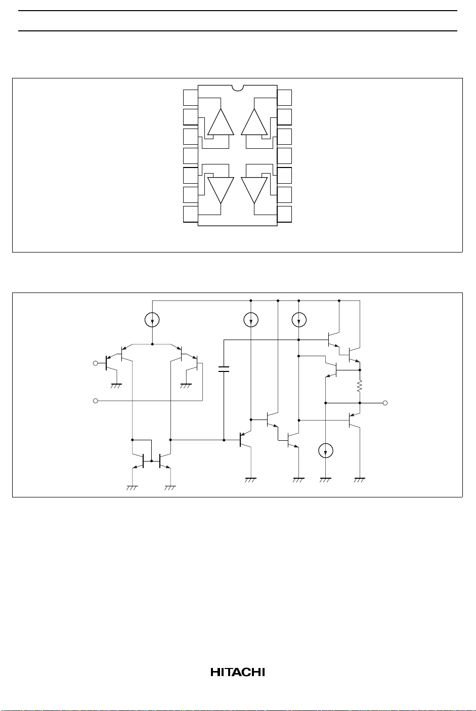
Pin Arrangement
Circuit Structure (1/4)
Q
Vin(–)
Vin(+)
Q
1
2
Vout1
Vin(–)1
Vin(+)1
V
CC
Vin(+)2
Vin(–)2
Vout2
Q
1
2
–+ +–
3
4
5
–+ +–
23
6
7
14
Vout4
13
12
11
10
9
8
Vin(–)4
Vin(+)4
GND
Vin(+)3
Vin(–)3
Vout3
41
(Top view)
Q
5
3
Q
4
C
Q
Q
6
7
R
1
Vout
Q
11
Q
10
Q
12
Q
13
Q
8
Q
9
2

Absolute Maximum Ratings (Ta = 25°C)
HA17902 Series
Item Symbol HA17902/PHA17902PJHA17902FPHA17902
FPJ
Power supply
V
CC
28 28 28 28 28 V
HA17902
FPK
Unit
voltage
Sink current Io sink 50 50 50 50 25 mA
Allowable power
P
T
625*
1
625*
1
625*
2
625*
2
625*
2
mW
dissipation
Common-mode
input voltage
Differential-mode
V
CM
–0.3 to
V
Vin(diff) ±V
–0.3 to
CC
CC
V
±V
CC
CC
–0.3 to
V
CC
±V
CC
–0.3 to
V
CC
±V
CC
–0.3 to
V
CC
±V
CC
V
V
input voltage
Operating
temperature
Storage
temperature
Topr –20 to +75 –40 to +85 –20 to +75 –40 to +85 –40 to
+125
Tstg –55 to
+125
–55 to
+125
–55 to
+125
–55 to
+125
–55 to
+150
°C
°C
Notes: 1. These are the allowable values up to Ta = 50°C. Derate by 8.3mW/°C above that temperature.
2. See notes on SOP Package Usage in Reliability section.
3

HA17902 Series
Electrical Characteristics 1 (VCC = + 15V, Ta = 25°C)
Item Symbol Min Typ Max Unit Test Conditions
Input offset voltage V
Input offset current I
Input bias current I
Power-supply
IO
IO
IB
PSRR — 93 — dB f = 100Hz, RS = 1kΩ, Rf = 100kΩ
—38mVV
— 5 50 nA IIO = | I
— 30 500 nA VCM = 7.5V
rejection ratio
Voltage gain A
Common-mode
VD
CMR — 80 — dB RS = 50Ω, Rf = 5kΩ
75 90 — dB RS = 1kΩ, Rf = 100kΩ, RL = ∞
rejection ratio
Common-mode input
V
CM
–0.3 — 13.5 V RS = 1kΩ, Rf = 100kΩ, f = 100Hz
voltage range
Maximum output
V
OP-P
— 13.6 — V f = 100Hz, RS = 1kΩ, Rf = 100kΩ,
voltage amplitude
Output voltage V
OH1
V
OH2
V
OL1
V
OL2
13.2 13.6 — V IOH = –1mA
12 13.3 — V IOH = –10mA
— 0.8 1 V IOL = 1mA
— 1.1 1.8 V IOL = 10mA
Output source current Io source 15 — — mA VOH = 10V
Output sink current Io sink 3 9 — mA VOL = 1V
Supply current I
CC
— 0.8 2 mA Vin = GND, RL = ∞
Slew rate SR — 0.19 — V/µs f = 1.5kHz, VCM = 7.5V, RL = ∞
Channel separation CS — 120 — dB f = 1kHz
= 7.5V, RS = 50Ω, Rf = 5kΩ
CM
–
+
– I
|, VCM = 7.5V
I
I
R
= 20kΩ
L
Electrical Characteristics 2 (VCC = + 15V, Ta = – 40 to 125°C)
Item Symbol Min Typ Max Unit Test Conditions
Input offset voltage V
Input offset current I
Input bias current I
Common-mode input
voltage range
Output voltage V
Supply current I
4
IO
IO
IB
V
CM
OH
V
OL
CC
——8 mVV
— — 200 nA VCM = 7.5V , IIO = | I
— — 500 nA VCM = 7.5V
0 — 13.0 V RS = 1kΩ, Rf = 100kΩ, f = 100Hz
13.0 ——VIOH = –1mA
——1.3VI
— — 4 mA Vin = GND, RL = ∞
= 7.5V, RS = 50Ω, Rf = 5kΩ
CM
= 1mA
OL
I
–
– I
+
|
I

HA17902 Series
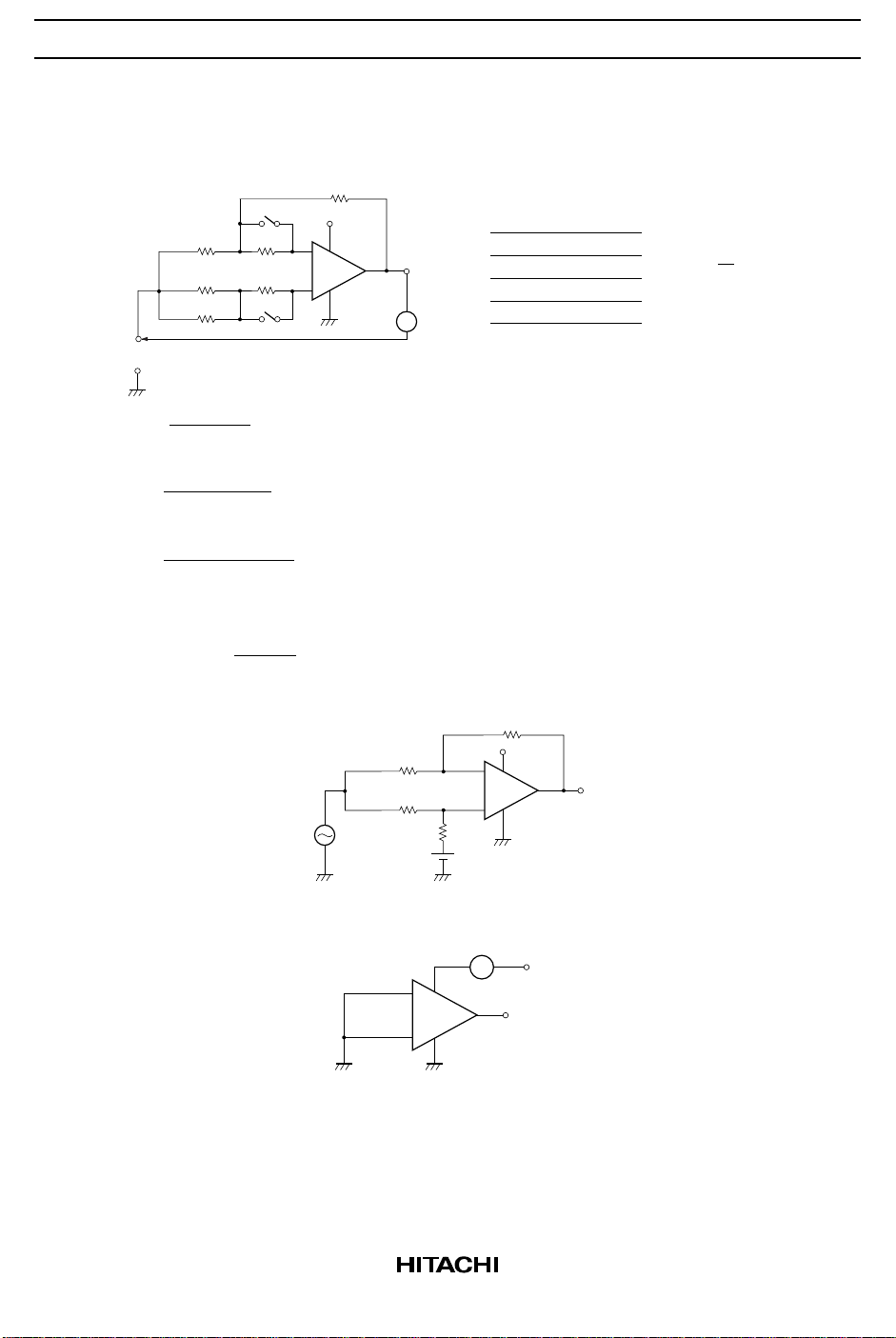
Test Circuits
1. Input offset voltage (VIO), input offset current (IIO), and Input bias current (IIB) test circuit
Rf 5k
V
CM
VIO =
1 + Rf / R
V
IIO =
R(1 + Rf / RS)
IIB =
2 · R(1 + Rf / R
R
S
R
S
Rf 5k
V
O2
| V
O4
50
50
O1
– V
– VO3 |
R 10k
R 10k
SW2
S
O1
SW1
)
S
V
–
+
(mV)
(nA)
(nA)
CC
V
Vout
SW1
On
Off
On
Off
SW2
On
Off
Off
On
V
O
V
O1
V
O2
V
O3
V
O4
VCM =
1
2
V
CC
2. Common-mode rejection ratio (CMR) test circuit
V
· Rf
CMR = 20 log
IN
V
· R
O
S
Vin
(dB)
R
50
S
50
R
S
3. Supply current (ICC) test circuit
–
+
Rf
5.0k
Rf 5.0k
–
+
A
V
CC
Vout
Vout
V
CC
5
 Loading...