HIT HA17901PJ, HA17901P, HA17901FPK, HA17901FPJ, HA17339F Datasheet
...
HA17901, HA17339 Series
Quadruple Comparators
Description
The HA17901 and HA17339 series products are comparators designed for use in power or control systems.
These IC operate from a single power-supply voltage over a wide range of voltages, and feature a reduced
power-supply current since the power-supply voltage is determined independently.
These comparators have the unique characteristic of ground being included in the common-mode input
voltage range, even when operating from a single-voltage power supply. These products have a wide range
of applications, including limit comparators, simple A/D converters, pulse/square-wave/time delay
generators, wide range VCO circuits, MOS clock timers, multivibrators, and high-voltage logic gates.
Features
• Wide power-supply voltage range: 2 to 36V
• Extremely low current drain: 0.8mA
• Low input bias current: 25nA
• Low input offset current: 5nA
• Low input offset voltage: 2mV
• The common-mode input voltage range includes ground.
• Low output saturation voltage: 1mV (5µA), 70mV (1mA)
• Output voltages compatible with CMOS logic systems

HA17901, HA17339 Series
Ordering Information
Type No. Application Package
HA17901PJ Car use DP-14
HA17901FPJ FP-14DA
HA17901FPK FP-14DA
HA17901P Industrial use DP-14
HA17901FP FP-14DA
HA17339 Commercial use DP-14
HA17339F FP-14DA
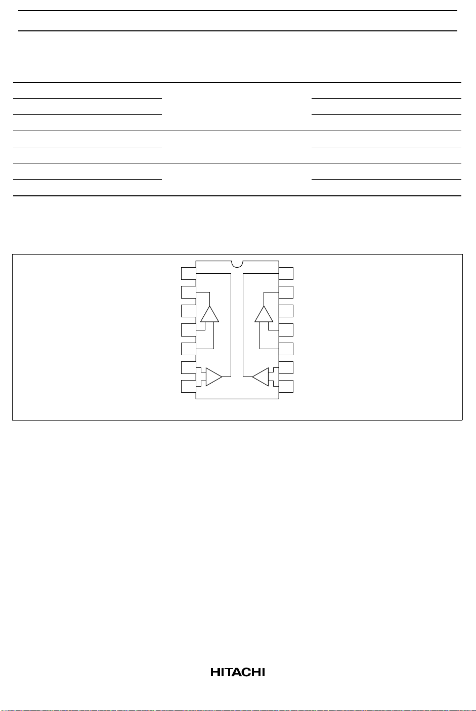
Pin Arrangement
Vout2
Vout1
V
CC
Vin(–)1
Vin(+)1
Vin(–)2
Vin(+)2
1
2
3
1
+
–
4
–
4
5
6
–
2
+
7
+
3
–
Vout3
14
Vout4
13
GND
12
+
Vin(+)4
11
Vin(–)4
10
Vin(+)3
9
Vin(–)3
8
(Top view)
2

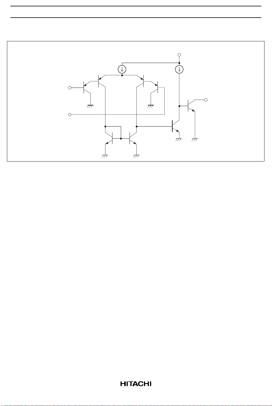
Circuit Structure (1/4)
HA17901, HA17339 Series
V
CC
Vin(–)
Q
2
Q
1
Q
3
Q
4Vin(+)
Vout
Q
8
Q
7
Q
5
Q
6
3

HA17901, HA17339 Series
Absolute Maximum Ratings (Ta = 25°C)
Item Symbol
Power-
V
CC
17901
P
36 36 36 36 36 36 36 V
17901
PJ
17901FP17901
FPJ
17901
FPK
17339 17339
F Unit
supply
voltage
Differential
Vin(diff) ±V
CC
±V
CC
±V
CC
±V
CC
±V
CC
±V
CC
±V
CC
V
input
voltage
Input
voltage
Output
Vin –0.3 to
+V
CC
2
Iout*
20 20 20 20 20 20 20 mA
–0.3 to
+V
CC
–0.3 to
+V
CC
–0.3 to
+V
CC
–0.3 to
+V
CC
–0.3 to
+V
CC
–0.3 to
+V
CC
V
current
Allowable
P
T
625*
1
625*
1
625*
3
625*
3
625*
3
625*
1
625*
3
mW
power
dissipation
Operating
temperature
Storage
temperature
Output pin
Topr –20 to
+75
Tstg –55 to
+125
–40 to
+85
–55 to
+125
–20 to
+75
–55 to
+125
–40 to
+85
–55 to
+125
–40 to
+125
–55 to
+150
–20 to
+75
–55 to
+125
–20 to
+75
–55 to
+125
Vout 36 36 36 36 36 36 36 V
°C
°C
voltage
Notes: 1. These are the allowable values up to Ta = 50°C. Derate by 8.3mW/°C above that temperature.
2. These products can be destroyed if the output and V
are shorted together. The maximum
CC
output current is the allowable value for continuous operation.
3. See notes of SOP Package Usage in Reliability section.
4

HA17901, HA17339 Series
Electrical Characteristics 1 (VCC = 5V, Ta = 25°C)
Item Symbol Min Typ Max Unit Test Condition
Input offset
V
IO
voltage
Input bias current I
Input offset
IB
I
IO
current
Common-mode
input voltage*
Supply current I
Voltage Gain A
Response time*2t
Output sink
V
1
CM
CC
VD
R
Iosink 6 16 — mA V
current
Output saturation
VO sat — 200 400 mV V
voltage
Output leakage
I
LO
current
Notes: 1. Voltages more negative than –0.3V are not allowed for the common-mode input voltage or for
either one of the input signal voltages.
2. The stipulated response time is the value for a 100 mV input step voltage that has a 5mV
overdrive.
— 2 7 mV Output switching point: when
V
= 1.4V, RS = 0Ω
O
— 25 250 nA I
— 5 50 nA I
0—V
– 1.5 V
CC
IN(+)
IN(+)
or I
– I
IN(–)
IN(–)
— 0.8 2 mA RL = ∞
— 200 — V/mV RL = 15kΩ
— 1.3 — µsVRL = 5V, RL = 5.1kΩ
= 1V, V
IN(–)
= 1V, V
IN(–)
= 0, VO ≤ 1.5V
IN(+)
= 0, Iosink =
IN(+)
3mA
— 0.1 — nA V
= 1V, V
IN(+)
= 0, VO = 5V
IN(–)
Electrical Characteristics 2 (VCC = 5V, Ta = – 41 to + 125°C)
Item Symbol Min Typ Max Unit Test Condition
Input offset
V
IO
voltage
Input offset
I
IO
current
Input bias current I
Common-mode
input voltage*
1
Output saturation
IB
V
VO
CM
sat
voltage
Output leakage
I
LO
current
Supply current I
CC
Note: 1. Voltages more negative than –0.3V are not allowed for the common-mode input voltage or for
either one of the input signal voltages.
— — 7 mV Output switching point: when
V
= 1.4V, RS = 0Ω
O
— — 200 nA I
IN(-)
– I
IN(+)
— — 500 nA
0—V
— — 440 mV V
– 2.0 V
CC
≥ 1V, V
IN(–)
= 0, Iosink ≤
IN(+)
4mA
— 1.0 — µAV
= 0V, V
IN(–)
≥ 1V, VO = 30V
IN(+)
— — 4.0 mA All comparators: RL = ∞,
All channels ON
5
 Loading...