

HA178M00 Series
3-terminal Fixed Voltage Regulators
Features
• Output current less than 500 mA
• Various output voltages: 5, 6, 7, 8, 9, 12, 15, 18, 20, and 24 V
• No external compensation circuit required
• Built-in current control circuit protects elements from destruction by short circuit
• Builting chip junction temperature limiting circuit protects elements from thermal destruction
• Builting internal power dissipation limiting circuit protects transistors in output stage
Ordering Information
Type Application Package
HA178M00PJ Series Automotive use TO - 220AB
HA178M00P Series Industrial use
HA178M00 Series Commercial use
Output Voltage Accuracy Grade
Type No. Grade Accuracy
HA178M05 None ±4
HA178M12 A ±2
B ±3
C +2, –4
HA178M00 Series
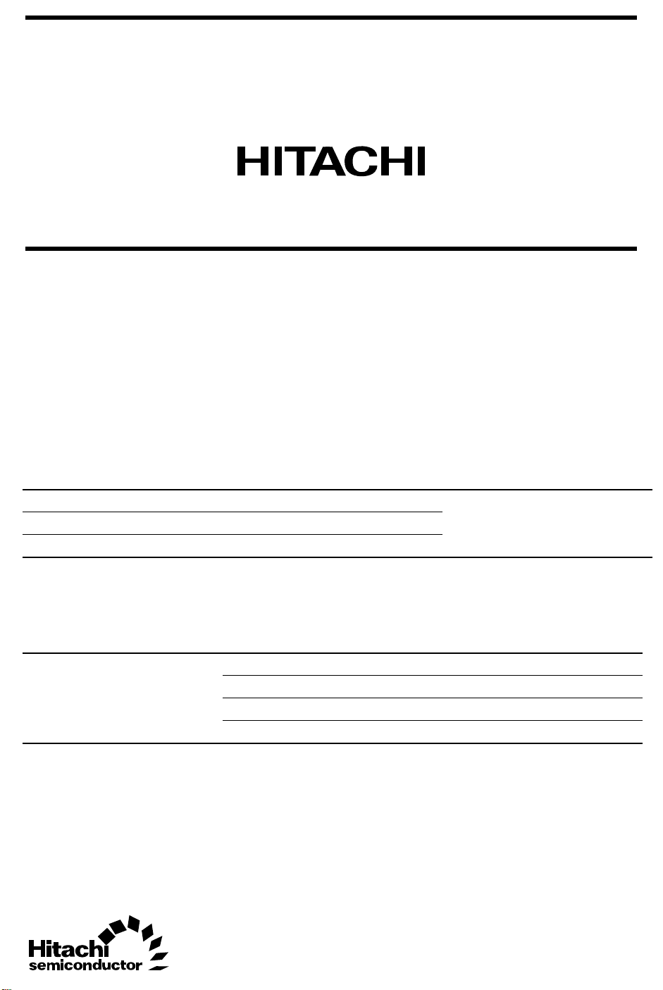
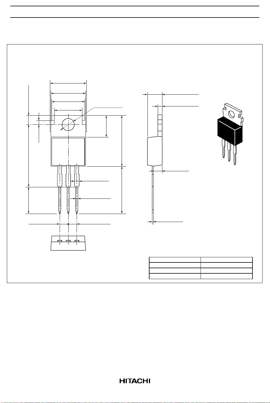
Pin Arrangement
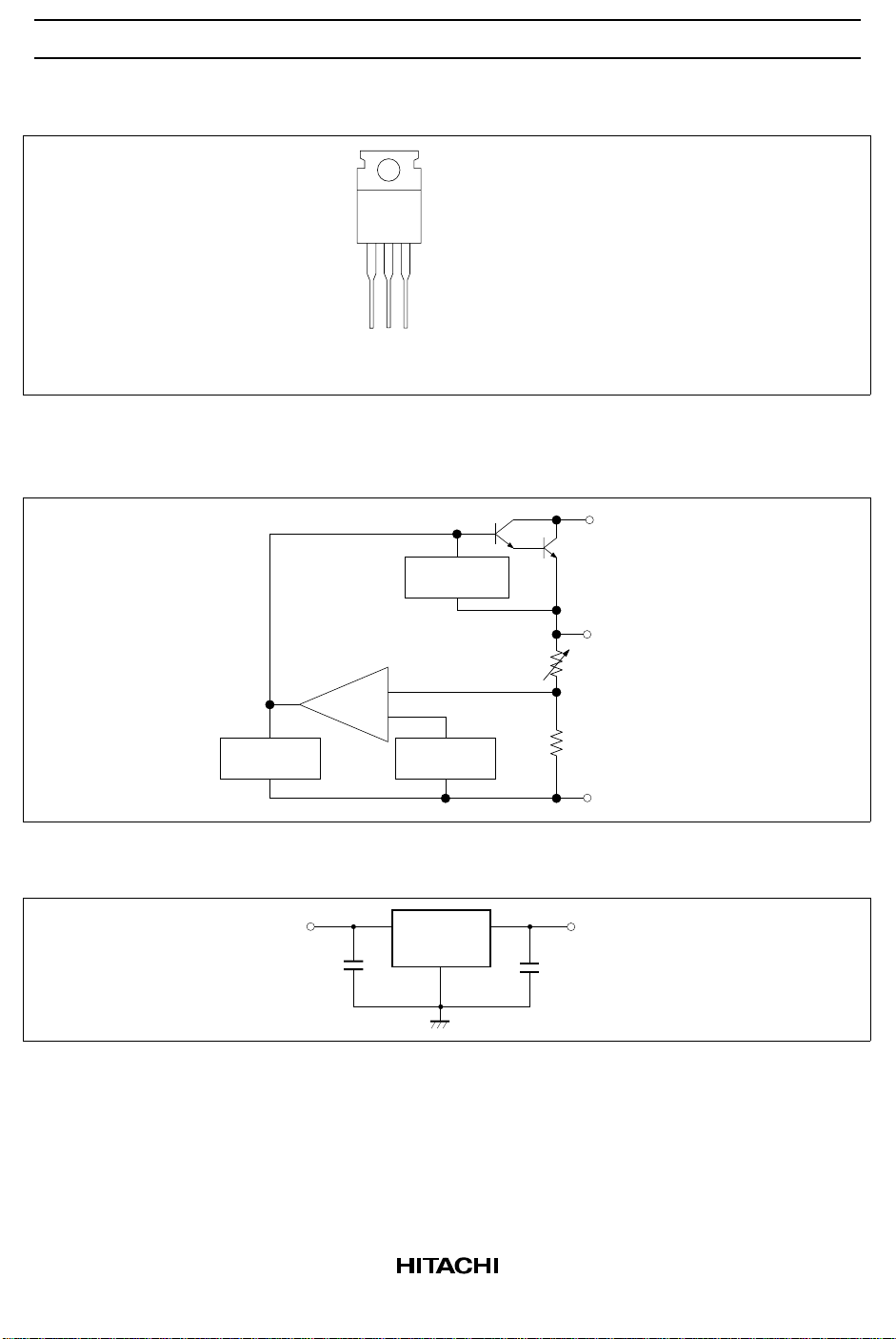
Block Diagram
4
Mark
1. Input
2. Common
3. Output
4. Common
123
(Top View)
INPUT
Over Current
Protection
Standard Circuit
Temperature
Protection
Input
0.33 F
C
Error
Amp.
1
Vref = 2.5 V
Reference
Voltage
HA178Mxx
C
0.1 Fµ
OUTPUT
COMMON
Output
2
µ
2
HA178M00 Series
Absolute Maximum Ratings (Ta = 25°C)
Item Symbol Rating Unit Notes
Input voltage V
Input voltage V
Power dissipation P
IN
IN
T
Operating temperature Topr –20 to +75 °C
Junction temperature Tj –20 to +125 °C
Storage temperature Tstg –55 to +125 °C
Notes: 1. For HA178M05P–HA178M18P, HA178M05–HA178M18
2. For HA178M20P, HA178M24P, HA178M20, HA178M24
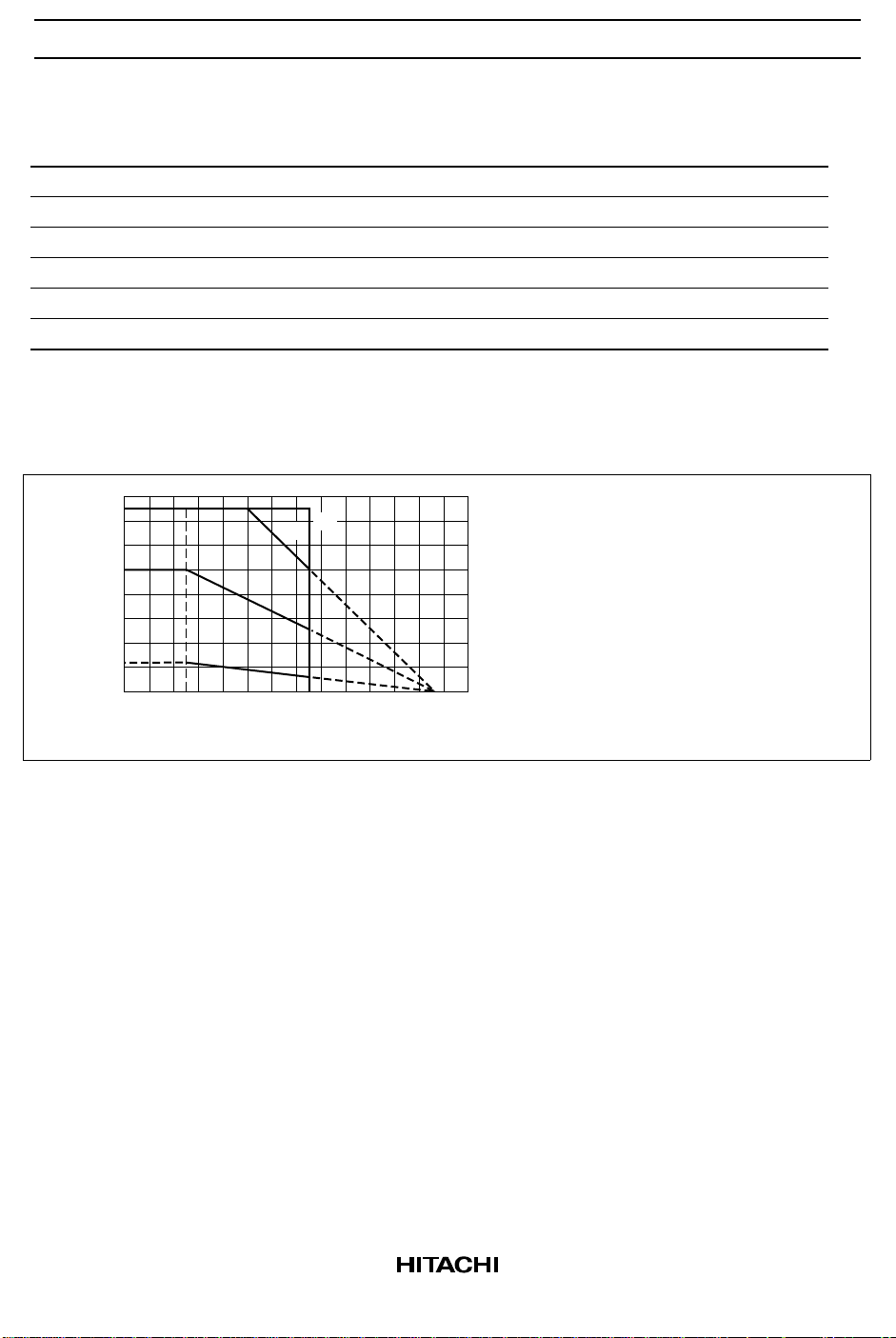
3. Follow derating curve
8
(1)
6
T
4
2
Max. Power
Dissipation P (max) (W)
0
20
40 60
(2)
(3)
(4)
80
Ambient Temperature Ta(°C)
35 V 1
40 V 2
7.5 W 3
(1) Infinite heat sink
(2) 5°C/W heat sink
(3) 15°C/W heat sink
(4) No heat sink
Thermal resistance
θjc = 3.0°C/W (typ)
5.0°C/W (max)
100
120
140
θja = 62°C/W (typ)
72°C/W (max)
Include fixed
)
thermal resistance
3
HA178M00 Series
HA178M05P/PJ, HA178M05 Electrical Characteristics (VIN = 10 V, I
0°C Tj 125°C, CIN = 0.33 µF, C
= 0.1 µF, unless otherwise specified)
OUT
= 350 mA,
OUT
Item Symbol Min Typ Max Unit Test Conditions
Output voltage V
OUT
4.8 5.0 5.2 V Tj = 25°C
4.75 — 5.25 7 V ≤ VIN ≤ 20 V,
Line regulation δV
O Line
5 mA ≤ I
— 3 100 mV Tj = 25°C 7 V ≤ VIN ≤ 25 V,
≤ 350 mA, PT ≤ 7.5 W
OUT
I
= 200 mA
OUT
— 1 50 8 V ≤ VIN ≤ 25 V,
I
= 200 mA
OUT
Load regulation δV
Quiescent current I
Quiescent current
δI
change
O Load
Q
Q
— 20 100 mV Tj = 25°C 5 mA ≤ I
— 10 50 5 mA ≤ I
— 4.5 6.0 mA Tj = 25°C, I
OUT
= 0
≤ 500 mA
OUT
≤ 200 mA
OUT
— — 0.8 mA 8 V ≤ VIN ≤ 25 V,
I
= 200 mA
OUT
— — 0.5 5 mA ≤ I
≤ 350 mA
OUT
Output noise voltage Vn — 40 — µV Ta = 25°C, 10 Hz ≤ f ≤ 100 kHz
Ripple rejection ratio R
REJ
Dropout voltage Vdrop — 2.0 — V I
Output short-circuit
I
OS
— 80 — dB f = 120 Hz I
— 80 — Tj = 25°CI
= 350 mA, Tj = 25°C
OUT
= 100 mA
OUT
= 300 mA
OUT
— 300 — mA Tj = 25°C, VIN = 35 V
current
Peak output current Io peak — 700 — mA Tj = 25°C
Temperature
δV
/δTj — –1.0 — mV/°CI
OUT
= 5 mA, 0°C ≤ Tj ≤ 125°C
OUT
coefficient of output
voltage
4

HA178M00 Series
HA178M06P/PJ, HA178M06 Electrical Characteristics (VIN = 11 V, I
0˚C Tj 125˚C, CIN = 0.33 µF, C
= 0.1 µF, unless otherwise specified)
OUT
= 350 mA,
OUT
Item Symbol Min Typ Max Unit Test Conditions
Output voltage V
OUT
5.75 6.0 6.25 V Tj = 25°C
5.7 — 6.3 8 V ≤ VIN ≤ 21 V,
Line regulation δV
O Line
5 mA ≤ I
— 5 120 mV Tj = 25°C 8 V ≤ VIN ≤ 25 V,
≤ 350 mA, PT ≤ 7.5 W
OUT
I
= 200 mA
OUT
— 1.5 60 9 V ≤ VIN ≤ 25 V,
I
= 200 mA
OUT
Load regulation δV
Quiescent current I
Quiescent current
δI
change
O Load
Q
Q
— 20 120 mV Tj = 25°C 5 mA ≤ I
— 10 60 5 mA ≤ I
— 4.5 6.0 mA Tj = 25°C, I
OUT
= 0
≤ 500 mA
OUT
≤ 200 mA
OUT
— — 0.8 mA 9 V ≤ VIN ≤ 25 V,
I
= 200 mA
OUT
— — 0.5 5 mA ≤ I
≤ 350 mA
OUT
Output noise voltage Vn — 45 — µV Ta = 25°C, 10 Hz ≤ f ≤ 100 kHz
Ripple rejection ratio R
REJ
Dropout voltage Vdrop — 2.0 — V I
Output short-circuit
I
OS
— 80 — dB f = 120 Hz I
— 80 — Tj = 25°CI
= 350 mA, Tj = 25°C
OUT
= 100 mA
OUT
= 300 mA
OUT
— 270 — mA Tj = 25°C, VIN = 35 V
current
Peak output current Io peak — 700 — mA Tj = 25°C
Temperature
δV
/δVj — –0.5 — mV/°CI
OUT
= 5 mA, 0°C ≤ Tj ≤ 125°C
OUT
coefficient of output
voltage
5

HA178M00 Series
HA178M07P/PJ, HA178M07 Electrical Characteristics (VIN = 12.5 V, I
0˚C Tj 125˚C, CIN = 0.33 µF, C
= 0.1 µF, unless otherwise specified)
OUT
= 350 mA,
OUT
Item Symbol Min Typ Max Unit Test Conditions
Output voltage V
OUT
6.72 7.0 7.28 V Tj = 25°C
6.65 — 7.35 9 V ≤ VIN ≤ 22 V,
Line regulation δV
O Line
5 mA ≤ I
— 5.5 140 mV Tj = 25°C 9 V ≤ VIN ≤ 25 V,
≤ 350 mA, PT ≤ 7.5 W
OUT
I
= 200 mA
OUT
— 1.7 70 10 V ≤ VIN ≤ 25 V,
I
= 200 mA
OUT
Load regulation δV
Quiescent current I
Quiescent current
δI
change
O Load
Q
Q
— 23 140 mV Tj = 25°C 5 mA ≤ I
— 10 70 5 mA ≤ I
— 4.6 6.0 mA Tj = 25°C, I
OUT
= 0
≤ 500 mA
OUT
≤ 200 mA
OUT
— — 0.8 mA 10 V ≤ VIN ≤ 25 V,
I
= 200 mA
OUT
— — 0.5 5 mA ≤ I
≤ 350 mA
OUT
Output noise voltage Vn — 48.5 — µV Ta = 25°C, 10 Hz ≤ f ≤ 100 kHz
Ripple rejection ratio R
REJ
Dropout voltage Vdrop — 2.0 — V I
Output short-circuit
I
OS
— 80 — dB f = 120 Hz I
— 80 — Tj = 25°CI
= 350 mA, Tj = 25°C
OUT
= 100 mA
OUT
= 300 mA
OUT
— 260 — mA Tj = 25°C, VIN = 35 V
current
Peak output current Io peak — 700 — mA Tj = 25°C
Temperature
δV
/δTj — –0.5 — mV/°CI
OUT
= 5 mA, 0°C ≤ Tj ≤ 125°C
OUT
coefficient of output
voltage
6

HA178M00 Series
HA178M08P/PJ, HA178M08 Electrical Characteristics (VIN = 14 V, I
0°C Tj 125°C, CIN = 0.33 µF, C
= 0.1 µF, unless otherwise specified)
OUT
= 350 mA,
OUT
Item Symbol Min Typ Max Unit Test Conditions
Output voltage V
OUT
7.7 8.0 8.3 V Tj = 25°C
7.6 — 8.4 10.5 V ≤ VIN ≤ 23 V,
Line regulation δV
O Line
5 mA ≤ I
— 6.0 160 mV Tj = 25°C 10.5 V ≤ VIN ≤ 25 V,
≤ 350 mA, PT ≤ 7.5 W
OUT
I
= 200 mA
OUT
— 2.0 80 11 V ≤ VIN ≤ 25 V,
I
= 200 mA
OUT
Load regulation δV
Quiescent current I
Quiescent current
δI
change
O Load
Q
Q
— 25 160 mV Tj = 25°C 5 mA ≤ I
— 10 80 5 mA ≤ I
— 4.6 6.0 mA Tj = 25°C, I
OUT
= 0
≤ 500 mA
OUT
≤ 200 mA
OUT
— — 0.8 mA 10.5 V ≤ VIN ≤ 25 V,
I
= 200 mA
OUT
— — 0.5 5 mA ≤ I
≤ 350 mA
OUT
Output noise voltage Vn — 52 — µV Ta = 25°C, 10 Hz ≤ f ≤ 100 kHz
Ripple rejection ratio R
REJ
Dropout voltage Vdrop — 2.0 — V I
Output short-circuit
I
OS
— 80 — dB f = 120 Hz I
— 80 — Tj = 25°CI
= 350 mA, Tj = 25°C
OUT
= 100 mA
OUT
= 300 mA
OUT
— 250 — mA Tj = 25°C, VIN = 35 V
current
Peak output current Io peak — 700 — mA Tj = 25°C
Temperature
δV
/δTj — –0.5 — mV/°CI
OUT
= 5 mA, 0°C ≤ Tj ≤ 125°C
OUT
coefficient of output
voltage
7

HA178M00 Series
HA178M09P/PJ, HA178M09 Electrical Characteristics (VIN = 15 V, I
0°C Tj 125°C, CIN = 0.33 µF, C
= 0.1 µF, unless otherwise specified)
OUT
= 350 mA,
OUT
Item Symbol Min Typ Max Unit Test Conditions
Output voltage V
OUT
8.64 9.0 9.36 V Tj = 25°C
8.55 — 9.45 11.5 V ≤ VIN ≤ 24 V,
Line regulation δV
O Line
5 mA ≤ I
— 7.0 180 mV Tj = 25°C 11.5 V ≤ VIN ≤ 25 V,
≤ 350 mA, PT ≤ 7.5 W
OUT
I
= 200 mA
OUT
— 2.5 90 12 V ≤ VIN ≤ 25 V
I
= 200 mA
OUT
Load regulation δV
Quiescent current I
Quiescent current
δI
change
O Load
Q
Q
— 25 200 mV Tj = 25°C 5 mA ≤ I
— 10 100 5 mA ≤ I
— 4.6 6.0 mA Tj = 25°C, I
OUT
= 0
≤ 500 mA
OUT
≤ 200 mA
OUT
— — 0.8 mA 12 V ≤ VIN ≤ 25 V,
I
= 200 mA
OUT
— — 0.5 5 mA ≤ I
≤ 350 mA
OUT
Output noise voltage Vn — 52 — µV Ta = 25°C, 10 Hz ≤ f ≤ 100 kHz
Ripple rejection ratio R
REJ
Dropout voltage Vdrop — 2.0 — V I
Output short-circuit
I
OS
— 80 — dB f = 120 Hz I
— 80 — Tj = 25°CI
= 350 mA, Tj = 25°C
OUT
= 100 mA
OUT
= 300 mA
OUT
— 250 — mA Tj = 25°C, VIN = 35 V
current
Peak output current Io peak — 700 — mA Tj = 25°C
Temperature
δV
/δTj — –0.9 — mV/°CI
OUT
= 5 mA, 0°C ≤ Tj ≤ 125°C
OUT
coefficient of output
voltage
8
HA178M00 Series
HA178M12P/PJ, HA178M12 Electrical Characteristics (VIN = 19 V, I
0°C Tj 125°C, CIN = 0.33 µF, C
= 0.1 µF, unless otherwise specified)
OUT
= = 350 mA,
OUT
Item Symbol Min Typ Max Unit Test Conditions
Output voltage V
OUT
11.5 12.0 12.5 V Tj = 25°C
11.4 — 12.6 14.5 V ≤ VIN ≤ 27 V,
Line regulation δV
O Line
5 mA ≤ I
— 10 240 mV Tj = 25°C 14.5 V ≤ VIN ≤ 30 V,
≤ 350 mA, PT ≤ 7.5 W
OUT
I
= 200 mA
OUT
— 3.0 120 16 V ≤ VIN ≤ 30 V,
I
= 200 mA
OUT
Load regulation δV
Quiescent current I
Quiescent current
δI
change
O Load
Q
Q
— 25 240 mV Tj = 25°C 5 mA ≤ I
— 10 120 5 mA ≤ I
— 4.8 6.0 mA Tj = 25°C, I
OUT
= 0
≤ 500 mA
OUT
≤ 200 mA
OUT
— — 0.8 mA 14.5 V ≤ VIN ≤ 30 V,
I
= 200 mA
OUT
— — 0.5 5 mA ≤ I
≤ 350 mA
OUT
Output noise voltage Vn — 75 — µV Ta = 25°C, 10 Hz ≤ f ≤ 100 kHz
Ripple rejection ratio R
REJ
Dropout voltage Vdrop — 2.0 — V I
Output short-circuit
I
OS
— 80 — dB f = 120 Hz I
— 80 — Tj = 25°CI
= 350 mA, Tj = 25°C
OUT
= 100 mA
OUT
= 300 mA
OUT
— 240 — mA Tj = 25°C, VIN = 35 V
current
Peak output curren Io peak — 700 — mA Tj = 25°C
Temperature
δV
/δTj — –1.0 — mV/°CI
OUT
= 5 mA, 0°C ≤ Tj ≤ 125°C
OUT
coefficient of output
voltage
9

HA178M00 Series
HA178M15P/PJ, HA178M15 Electrical Characteristics (VIN = 23 V, I
0°C Tj 125°C, CIN = 0.33 µF, C
= 0.1 µF, unless otherwise specified)
OUT
= 350 mA,
OUT
Item Symbol Min Typ Max Unit Test Conditions
Output voltage V
OUT
14.4 15.0 15.6 V Tj = 25°C
14.25 — 15.75 17.5 V ≤ VIN ≤ 30 V,
Line regulation δV
O Line
5 mA ≤ I
— 11 300 mV Tj = 25°C 17.5 V ≤ VIN ≤ 30 V,
≤ 350 mA, PT ≤ 7.5 W
OUT
I
= 200 mA
OUT
— 3.0 150 20 V ≤ VIN ≤ 30 V,
I
= 200 mA
OUT
Load regulation δV
Quiescent current I
Quiescent current
δI
change
O Load
Q
Q
— 25 300 mV Tj = 25°C 5 mA ≤ I
— 10 150 5 mA ≤ I
— 4.8 6.0 mA Tj = 25°C, I
OUT
= 0
≤ 500 mA
OUT
≤ 200 mA
OUT
— — 0.8 mA 17.5 V ≤ VIN ≤ 30 V,
I
= 200 mA
OUT
— — 0.5 5 mA ≤ I
≤ 350 mA
OUT
Output noise voltage Vn — 90 — µV Ta = 25°C, 10 Hz ≤ f ≤ 100 kHz
Ripple rejection ratio R
REJ
Dropout voltage Vdrop — 2.0 — V I
Output short-circuit
I
OS
— 70 — dB f = 120 Hz I
— 70 — Tj = 25°CI
= 350 mA, Tj = 25°C
OUT
= 100 mA
OUT
= 300 mA
OUT
— 240 — mA Tj = 25°C, VIN = 35 V
current
Peak output current Io peak — 700 — mA Tj = 25°C
Temperature
δV
/δTj — –1.0 — mV/°CI
OUT
= 5 mA, 0°C ≤ Tj ≤ 125°C
OUT
coefficient of output
voltage
10

HA178M00 Series
HA178M18P/PJ, HA178M18 Electrical Characteristics (VIN = 27 V, I
0°C Tj 125°C, CIN = 0.33 µF, C
= 0.1 µF, unless otherwise specified)
OUT
= 350 mA,
OUT
Item Symbol Min Typ Max Unit Test Conditions
Output voltage V
OUT
17.3 18.0 18.7 V Tj = 25°C
17.1 — 18.9 21 V ≤ VIN ≤ 33 V,
Line regulation dV
O Line
5 mA ≤ I
— 15 360 mV Tj = 25°C 21 V ≤ VIN ≤ 33 V,
≤ 350 mA, PT ≤ 7.5 W
OUT
I
= 200 mA
OUT
— 5.0 180 24 V ≤ VIN ≤ 33 V,
I
= 200 mA
OUT
Load regulation δV
Quiescent current I
Quiescent current
δI
change
O Load
Q
Q
— 25 360 mV Tj = 25°C 5 mA ≤ I
— 10 180 5 mA ≤ I
— 4.8 6.0 mA Tj = 25°C, I
OUT
= 0
≤ 500 mA
OUT
≤ 200 mA
OUT
— — 0.8 mA 21 V ≤ VIN ≤ 35 V,
I
= 200 mA
OUT
— — 0.5 5 mA ≤ I
≤ 350 mA
OUT
Output noise voltage Vn — 110 — µV Ta = 25°C, 10 Hz ≤ f ≤ 100 kHz
Ripple rejection ratio R
REJ
Dropout voltage Vdrop — 2.0 — V I
Output short-circuit
I
OS
— 70 — dB f = 120 Hz I
— 70 — Tj = 25°CI
= 350 mA, Tj = 25°C
OUT
= 100 mA
OUT
= 300 mA
OUT
— 240 — mA Tj = 25°C, VIN = 35 V
current
Peak output current Io peak — 700 — mA Tj = 25°C
Temperature
δV
/δTj — –1.0 — mV/°CI
OUT
= 5 mA, 0°C ≤ Tj ≤ 125°C
OUT
coefficient of output
voltage
11

HA178M00 Series
HA178M20P/PJ, HA178M20 Electrical Characteristics (VIN = 29 V, I
0°C Tj 125°C, CIN = 0.33 µF, C
= 0.1 µF, unless otherwise specified)
OUT
= 350 mA,
OUT
Item Symbol Min Typ Max Unit Test Conditions
Output voltage V
OUT
19.2 20 20.8 V Tj = 25°C
19 — 21 23 V ≤ VIN ≤ 35 V,
Line regulation δV
O Line
5 mA ≤ I
— 17 400 mV Tj = 25°C 23 V ≤ VIN ≤ 35 V,
≤ 350 mA, PT ≤ 7.5 W
OUT
I
= 200 mA
OUT
— 6.0 200 24 V ≤ VIN ≤ 35 V,
I
= 200 mA
OUT
Load regulation δV
Quiescent current I
Quiescent current
δI
change
O Load
Q
Q
— 30 400 mV Tj = 25°C 5 mA ≤ I
— 10 200 5 mA ≤ I
— 4.9 6.0 mA Tj = 25°C, I
OUT
= 0
≤ 500 mA
OUT
≤ 200 mA
OUT
— — 0.8 mA 23 V ≤ VIN ≤ 35 V,
I
= 200 mA
OUT
— — 0.5 5 mA ≤ I
≤ 350 mA
OUT
Output noise voltage Vn — 110 — µV Ta = 25°C, 10 Hz ≤ f ≤ 100 kHz
Ripple rejection ratio R
REJ
Dropout voltage Vdrop — 2.0 — V I
Output short-circuit
I
OS
— 70 — dB f = 120 Hz I
— 70 — Tj = 25°CI
= 350 mA, Tj = 25°C
OUT
= 100 mA
OUT
= 300 mA
OUT
— 240 — mA Tj = 25°C, VIN = 35 V
current
Peak output current Io peak — 700 — mA Tj = 25°C
Temperature
δV
/δTj — –1.1 — mV/°CI
OUT
= 5 mA, 0°C ≤ Tj ≤ 125°C
OUT
coefficient of output
voltage
12

HA178M00 Series
HA178M24P/PJ, HA178M24 Electrical Characteristics (VIN = 33 V, I
0°C Tj 125°C, CIN = 0.33 µF, C
= 0.1 µF, unless otherwise specified)
OUT
= 350 mA,
OUT
Item Symbol Min Typ Max Unit Test Conditions
Output voltage V
OUT
23.0 24.0 25.0 V Tj = 25°C
22.8 — 25.2 27 V ≤ VIN ≤ 38 V,
Line regulation δV
O Line
5 mA ≤ I
— 18 480 mV Tj = 25°C 27 V ≤ VIN ≤ 38 V,
≤ 350 mA, PT ≤ 7.5 W
OUT
I
= 200 mA
OUT
— 6.0 240 28 V ≤ VIN ≤ 38 V,
I
= 200 mA
OUT
Load regulation δV
Quiescent current I
Quiescent current
δI
change
O Load
Q
Q
— 30 480 mV Tj = 25°C 5 mA ≤ I
— 10 240 5 mA ≤ I
— 5.0 8.0 mA Tj = 25°C, I
OUT
= 0
≤ 500 mA
OUT
≤ 200 mA
OUT
— — 0.8 mA 27 V ≤ VIN ≤ 38 V,
I
= 200 mA
OUT
— — 0.5 5 mA ≤ I
≤ 350 mA
OUT
Output noise voltage Vn — 170 — µV Ta = 25°C, 10 Hz ≤ f ≤ 100 kHz
Ripple rejection ratio R
REJ
Dropout voltage Vdrop — 2.0 — V I
Output short-circuit
I
OS
— 70 — dB f = 120 Hz I
— 70 — Tj = 25°CI
= 350 mA, Tj = 25°C
OUT
= 100 mA
OUT
= 300 mA
OUT
— 240 — mA Tj = 25°C, VIN = 35 V
current
Peak output current Io peak — 700 — mA Tj = 25°C
Temperature coefficient
δV
/δTj — –1.2 — mV/°CI
OUT
= 5 mA, 0°C ≤ Tj ≤ 125°C
OUT
of output voltage
13

HA178M00 Series
Characteristic Curves
Output Voltage vs. Operating
Junction Temperature (1)
5.2
HA178M05
V
IN
Iout = 5mA
5.0
Output Voltage Vout (V)
4.8
0 25 50 75 100 125
Operating Junction Temperature Tj (°C)
Output Voltage vs. Output Current
30
HA178M24
V
20
HA178M15
VIN = 23 V
10
Output Voltage Vout (V)
HA178M05
VIN = 10 V
0
0 0.5 1.0 1.5
Output Current Iout (A)
= 10 V
= 33 V
IN
Ta = 25°C
Ripple Rejection Ratio vs. Frequency
80
(dB)
REJ
Iout = 300 mA
60
40
Ripple Rejection Ratio R
100 1 k 10 k 100 k
Frequency f (Hz)
Peak Output Current vs. Dropout Voltage
1.5
(A)
OP
HA178M05
Tj = 25°C
1.0
0.5
Peak Output Current I
0
0102030
Dropout Voltage V
DROP
(V)
Output Voltage vs. Input Voltage (1)
10
5
Output Voltage Vout (V)
0
010203040
14
Iout = 0.5 A
0.35 A
0.1 A
Input Voltage V
IN
(V)
HA178M05
Tj = 25°C
Output Voltage vs. Input Voltage (2)
25
20
15
Iout = 500 mA
Tj = 25°C
HA178M24
HA178M15
10
5
Output Voltage Vout (V)
HA178M05
0
0 10203040
Input Voltage V
(V)
IN

HA178M00 Series
Quiescent Operating Current vs.
Input Voltage
6
5
4
3
(mA)
Q
I
2
HA178M05
Iout = 0 mA
Tj = 25°C
1
Quiescent Operating Current
0
010203040
Input Voltage V
IN
(V)
Output Voltage vs. Operating
Junction Temperature (3)
25.0
HA178M24
V
= 33 V
IN
Iout = 5 mA
24.0
Output Voltage vs. Operating
Junction Temperature (2)
15.6
HA178M15
V
IN
Iout = 5 mA
15.0
Output Voltage Vout (V)
14.4
0 25 50 75 100 125
Operating Junction Temperature Tj (°C)
= 23 V
Output Voltage Vout (V)
23.0
0 25 50 75 100 125
Operating Junction Temperature Tj (°C)
15
HA178M00 Series
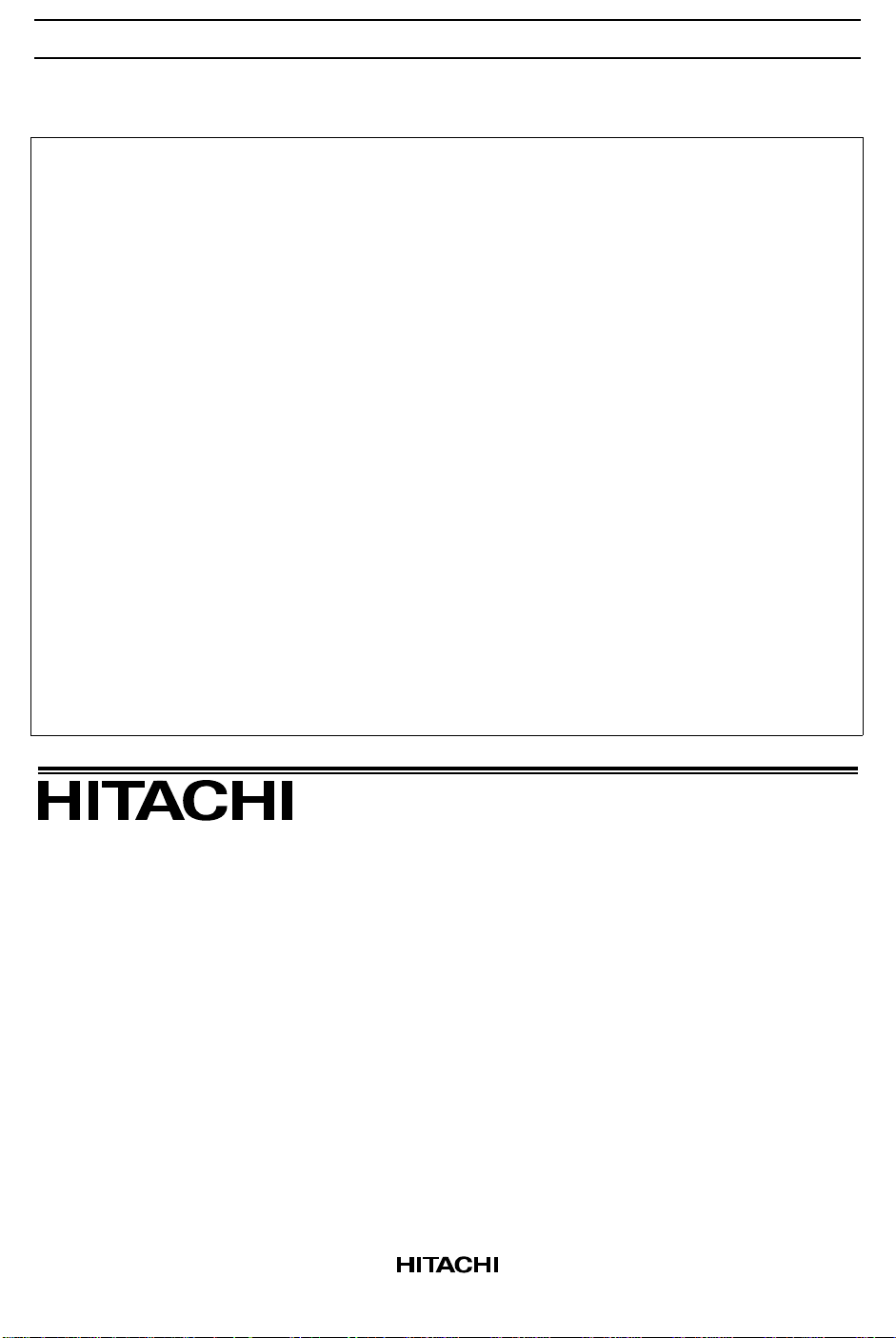
Package Dimensions
11.5 MAX
Unit: mm
2.79 ± 0.218.5 ± 0.57.8 ± 0.5
1.27
2.54 ± 0.5
10.16 ± 0.2
9.5
8.0
φ 3.6
-0.08
1.5 MAX
0.76 ± 0.1
2.54 ± 0.5
+0.2
6.4
–0.1
+0.1
4.44 ± 0.2
1.26 ± 0.15
2.7 MAX
14.0 ± 0.5 15.0 ± 0.3
0.5 ± 0.1
16
Hitachi Code
JEDEC
EIAJ
Mass
(reference value)
TO-220AB
Conforms
Conforms
1.8 g
HA178M00 Series
Cautions
1. Hitachi neither warrants nor grants licenses of any rights of Hitachi’s or any third party’s patent,
copyright, trademark, or other intellectual property rights for information contained in this document.
Hitachi bears no responsibility for problems that may arise with third party’s rights, including
intellectual property rights, in connection with use of the information contained in this document.
2. Products and product specifications may be subject to change without notice. Confirm that you have
received the latest product standards or specifications before final design, purchase or use.
3. Hitachi makes every attempt to ensure that its products are of high quality and reliability. However,
contact Hitachi’s sales office before using the product in an application that demands especially high
quality and reliability or where its failure or malfunction may directly threaten human life or cause risk
of bodily injury, such as aerospace, aeronautics, nuclear power, combustion control, transportation,
traffic, safety equipment or medical equipment for life support.
4. Design your application so that the product is used within the ranges guaranteed by Hitachi particularly
for maximum rating, operating supply voltage range, heat radiation characteristics, installation
conditions and other characteristics. Hitachi bears no responsibility for failure or damage when used
beyond the guaranteed ranges. Even within the guaranteed ranges, consider normally foreseeable
failure rates or failure modes in semiconductor devices and employ systemic measures such as failsafes, so that the equipment incorporating Hitachi product does not cause bodily injury, fire or other
consequential damage due to operation of the Hitachi product.
5. This product is not designed to be radiation resistant.
6. No one is permitted to reproduce or duplicate, in any form, the whole or part of this document without
written approval from Hitachi.
7. Contact Hitachi’s sales office for any questions regarding this document or Hitachi semiconductor
products.
Hitachi, Ltd.
Semiconductor & Integrated Circuits.
Nippon Bldg., 2-6-2, Ohte-machi, Chiyoda-ku, Tokyo 100-0004, Japan
Tel: Tokyo (03) 3270-2111 Fax: (03) 3270-5109
URL NorthAmerica : http:semiconductor.hitachi.com/
For further information write to:
Hitachi Semiconductor
(America) Inc.
179 East Tasman Drive,
San Jose,CA 95134
Tel: <1> (408) 433-1990
Fax: <1>(408) 433-0223
Europe : http://www.hitachi-eu.com/hel/ecg
Asia (Singapore) : http://www.has.hitachi.com.sg/grp3/sicd/index.htm
Asia (Taiwan) : http://www.hitachi.com.tw/E/Product/SICD_Frame.htm
Asia (HongKong) : http://www.hitachi.com.hk/eng/bo/grp3/index.htm
Japan : http://www.hitachi.co.jp/Sicd/indx.htm
Hitachi Europe GmbH
Electronic components Group
Dornacher Straβe 3
D-85622 Feldkirchen, Munich
Germany
Tel: <49> (89) 9 9180-0
Fax: <49> (89) 9 29 30 00
Hitachi Europe Ltd.
Electronic Components Group.
Whitebrook Park
Lower Cookham Road
Maidenhead
Berkshire SL6 8YA, United Kingdom
Tel: <44> (1628) 585000
Fax: <44> (1628) 778322
Hitachi Asia Pte. Ltd.
16 Collyer Quay #20-00
Hitachi Tower
Singapore 049318
Tel: 535-2100
Fax: 535-1533
Hitachi Asia Ltd.
Taipei Branch Office
3F, Hung Kuo Building. No.167,
Tun-Hwa North Road, Taipei (105)
Tel: <886> (2) 2718-3666
Fax: <886> (2) 2718-8180
Copyright ' Hitachi, Ltd., 1998. All rights reserved. Printed in Japan.
Hitachi Asia (Hong Kong) Ltd.
Group III (Electronic Components)
7/F., North Tower, World Finance Centre,
Harbour City, Canton Road, Tsim Sha Tsui,
Kowloon, Hong Kong
Tel: <852> (2) 735 9218
Fax: <852> (2) 730 0281
Telex: 40815 HITEC HX
17
 Loading...