HIT HA178M20P, HA178M20, HA178M18P, HA178M18, HA178M15P Datasheet
...
HA178M00 Series
3-terminal Fixed Voltage Regulators
Features
• Output current less than 500 mA
• Various output voltages: 5, 6, 7, 8, 9, 12, 15, 18, 20, and 24 V
• No external compensation circuit required
• Built-in current control circuit protects elements from destruction by short circuit
• Builting chip junction temperature limiting circuit protects elements from thermal destruction
• Builting internal power dissipation limiting circuit protects transistors in output stage
Ordering Information
Type Application Package
HA178M00PJ Series Automotive use TO - 220AB
HA178M00P Series Industrial use
HA178M00 Series Commercial use
Output Voltage Accuracy Grade
Type No. Grade Accuracy
HA178M05 None ±4
HA178M12 A ±2
B ±3
C +2, –4

HA178M00 Series
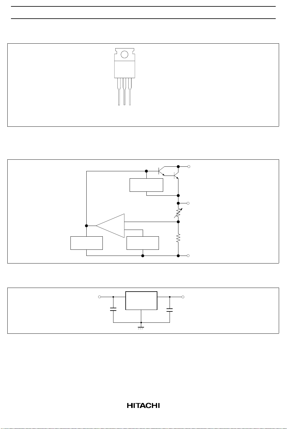
Pin Arrangement
Block Diagram
4
Mark
1. Input
2. Common
3. Output
4. Common
123
(Top View)
INPUT
Over Current
Protection
Standard Circuit
Temperature
Protection
Input
0.33 F
C
Error
Amp.
1
Vref = 2.5 V
Reference
Voltage
HA178Mxx
C
0.1 Fµ
OUTPUT
COMMON
Output
2
µ
2

HA178M00 Series
Absolute Maximum Ratings (Ta = 25°C)
Item Symbol Rating Unit Notes
Input voltage V
Input voltage V
Power dissipation P
IN
IN
T
Operating temperature Topr –20 to +75 °C
Junction temperature Tj –20 to +125 °C
Storage temperature Tstg –55 to +125 °C
Notes: 1. For HA178M05P–HA178M18P, HA178M05–HA178M18
2. For HA178M20P, HA178M24P, HA178M20, HA178M24
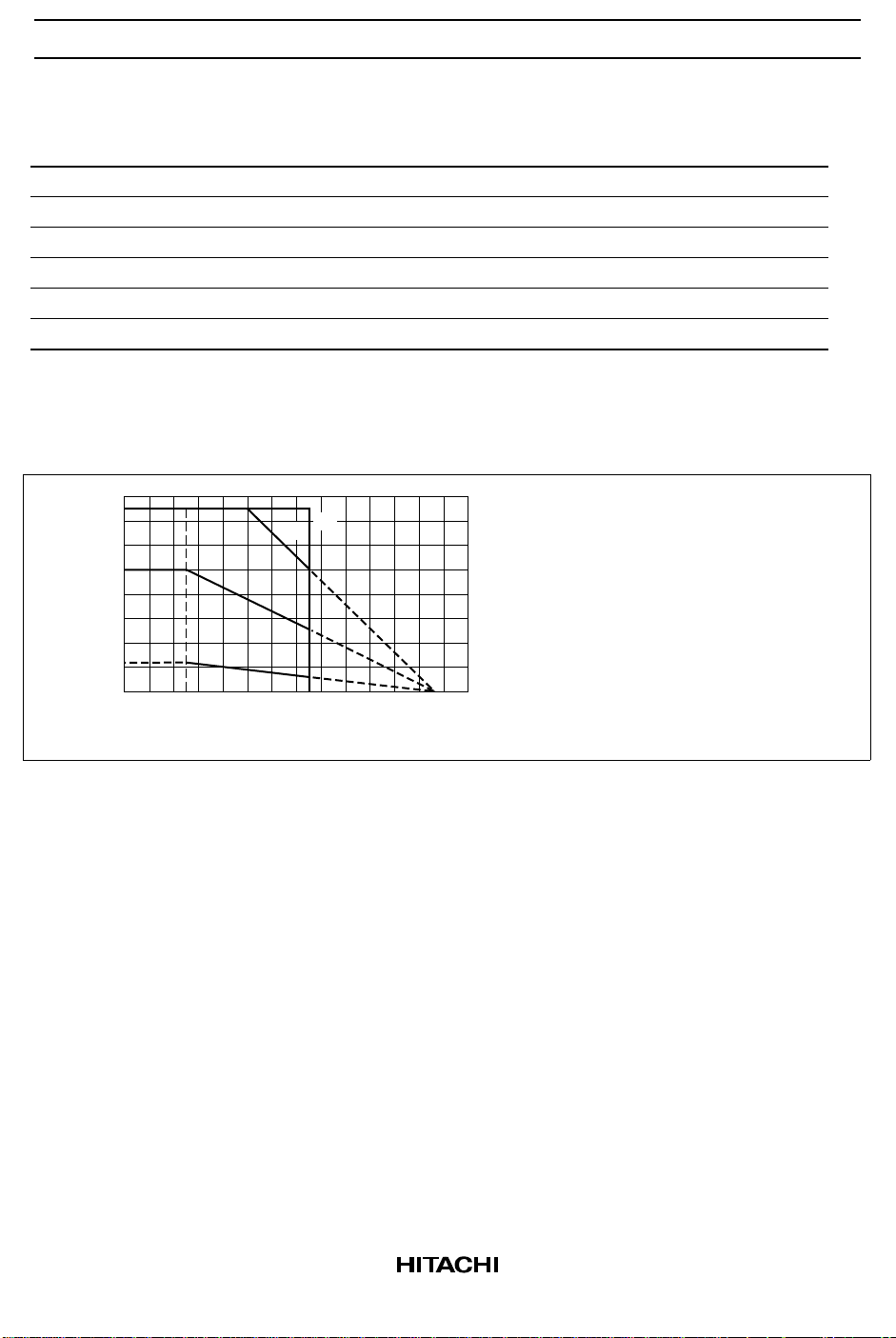
3. Follow derating curve
8
(1)
6
T
4
2
Max. Power
Dissipation P (max) (W)
0
20
40 60
(2)
(3)
(4)
80
Ambient Temperature Ta(°C)
35 V 1
40 V 2
7.5 W 3
(1) Infinite heat sink
(2) 5°C/W heat sink
(3) 15°C/W heat sink
(4) No heat sink
Thermal resistance
θjc = 3.0°C/W (typ)
5.0°C/W (max)
100
120
140
θja = 62°C/W (typ)
72°C/W (max)
Include fixed
)
thermal resistance
3

HA178M00 Series
HA178M05P/PJ, HA178M05 Electrical Characteristics (VIN = 10 V, I
0°C Tj 125°C, CIN = 0.33 µF, C
= 0.1 µF, unless otherwise specified)
OUT
= 350 mA,
OUT
Item Symbol Min Typ Max Unit Test Conditions
Output voltage V
OUT
4.8 5.0 5.2 V Tj = 25°C
4.75 — 5.25 7 V ≤ VIN ≤ 20 V,
Line regulation δV
O Line
5 mA ≤ I
— 3 100 mV Tj = 25°C 7 V ≤ VIN ≤ 25 V,
≤ 350 mA, PT ≤ 7.5 W
OUT
I
= 200 mA
OUT
— 1 50 8 V ≤ VIN ≤ 25 V,
I
= 200 mA
OUT
Load regulation δV
Quiescent current I
Quiescent current
δI
change
O Load
Q
Q
— 20 100 mV Tj = 25°C 5 mA ≤ I
— 10 50 5 mA ≤ I
— 4.5 6.0 mA Tj = 25°C, I
OUT
= 0
≤ 500 mA
OUT
≤ 200 mA
OUT
— — 0.8 mA 8 V ≤ VIN ≤ 25 V,
I
= 200 mA
OUT
— — 0.5 5 mA ≤ I
≤ 350 mA
OUT
Output noise voltage Vn — 40 — µV Ta = 25°C, 10 Hz ≤ f ≤ 100 kHz
Ripple rejection ratio R
REJ
Dropout voltage Vdrop — 2.0 — V I
Output short-circuit
I
OS
— 80 — dB f = 120 Hz I
— 80 — Tj = 25°CI
= 350 mA, Tj = 25°C
OUT
= 100 mA
OUT
= 300 mA
OUT
— 300 — mA Tj = 25°C, VIN = 35 V
current
Peak output current Io peak — 700 — mA Tj = 25°C
Temperature
δV
/δTj — –1.0 — mV/°CI
OUT
= 5 mA, 0°C ≤ Tj ≤ 125°C
OUT
coefficient of output
voltage
4

HA178M00 Series
HA178M06P/PJ, HA178M06 Electrical Characteristics (VIN = 11 V, I
0˚C Tj 125˚C, CIN = 0.33 µF, C
= 0.1 µF, unless otherwise specified)
OUT
= 350 mA,
OUT
Item Symbol Min Typ Max Unit Test Conditions
Output voltage V
OUT
5.75 6.0 6.25 V Tj = 25°C
5.7 — 6.3 8 V ≤ VIN ≤ 21 V,
Line regulation δV
O Line
5 mA ≤ I
— 5 120 mV Tj = 25°C 8 V ≤ VIN ≤ 25 V,
≤ 350 mA, PT ≤ 7.5 W
OUT
I
= 200 mA
OUT
— 1.5 60 9 V ≤ VIN ≤ 25 V,
I
= 200 mA
OUT
Load regulation δV
Quiescent current I
Quiescent current
δI
change
O Load
Q
Q
— 20 120 mV Tj = 25°C 5 mA ≤ I
— 10 60 5 mA ≤ I
— 4.5 6.0 mA Tj = 25°C, I
OUT
= 0
≤ 500 mA
OUT
≤ 200 mA
OUT
— — 0.8 mA 9 V ≤ VIN ≤ 25 V,
I
= 200 mA
OUT
— — 0.5 5 mA ≤ I
≤ 350 mA
OUT
Output noise voltage Vn — 45 — µV Ta = 25°C, 10 Hz ≤ f ≤ 100 kHz
Ripple rejection ratio R
REJ
Dropout voltage Vdrop — 2.0 — V I
Output short-circuit
I
OS
— 80 — dB f = 120 Hz I
— 80 — Tj = 25°CI
= 350 mA, Tj = 25°C
OUT
= 100 mA
OUT
= 300 mA
OUT
— 270 — mA Tj = 25°C, VIN = 35 V
current
Peak output current Io peak — 700 — mA Tj = 25°C
Temperature
δV
/δVj — –0.5 — mV/°CI
OUT
= 5 mA, 0°C ≤ Tj ≤ 125°C
OUT
coefficient of output
voltage
5

HA178M00 Series
HA178M07P/PJ, HA178M07 Electrical Characteristics (VIN = 12.5 V, I
0˚C Tj 125˚C, CIN = 0.33 µF, C
= 0.1 µF, unless otherwise specified)
OUT
= 350 mA,
OUT
Item Symbol Min Typ Max Unit Test Conditions
Output voltage V
OUT
6.72 7.0 7.28 V Tj = 25°C
6.65 — 7.35 9 V ≤ VIN ≤ 22 V,
Line regulation δV
O Line
5 mA ≤ I
— 5.5 140 mV Tj = 25°C 9 V ≤ VIN ≤ 25 V,
≤ 350 mA, PT ≤ 7.5 W
OUT
I
= 200 mA
OUT
— 1.7 70 10 V ≤ VIN ≤ 25 V,
I
= 200 mA
OUT
Load regulation δV
Quiescent current I
Quiescent current
δI
change
O Load
Q
Q
— 23 140 mV Tj = 25°C 5 mA ≤ I
— 10 70 5 mA ≤ I
— 4.6 6.0 mA Tj = 25°C, I
OUT
= 0
≤ 500 mA
OUT
≤ 200 mA
OUT
— — 0.8 mA 10 V ≤ VIN ≤ 25 V,
I
= 200 mA
OUT
— — 0.5 5 mA ≤ I
≤ 350 mA
OUT
Output noise voltage Vn — 48.5 — µV Ta = 25°C, 10 Hz ≤ f ≤ 100 kHz
Ripple rejection ratio R
REJ
Dropout voltage Vdrop — 2.0 — V I
Output short-circuit
I
OS
— 80 — dB f = 120 Hz I
— 80 — Tj = 25°CI
= 350 mA, Tj = 25°C
OUT
= 100 mA
OUT
= 300 mA
OUT
— 260 — mA Tj = 25°C, VIN = 35 V
current
Peak output current Io peak — 700 — mA Tj = 25°C
Temperature
δV
/δTj — –0.5 — mV/°CI
OUT
= 5 mA, 0°C ≤ Tj ≤ 125°C
OUT
coefficient of output
voltage
6
 Loading...