

HIT HA178L56UA, HA178L56P, HA178L15UA, HA178L15P, HA178L15 Datasheet
...
HA178L00 Series
3-terminal Fixed Voltage Regulators
Description
The HA178L00 series three-terminal fixed output voltage regulators. Can be used not only as stabilized
power sources, but also as Zener diodes because of their small outline package.
Features
• Maximum output current: 150 mA (Tj= 25°C)
• Large maximum power dissipation: 800 mW
• Overcurrent protection
• Temperature protection circuit
Ordering Information
Application
Standard Output Voltage
Tolerance ±8%
A Version Output Voltage
Tolerance ±5%
Industrial use HA178L00P HA178L00PA
Commercial use HA178L00 HA178L00A
HA178L00UA

HA178L00 Series
2
Output Voltage and Type
HA178L00PA • HA178L00P • HA178L00A • HA178L00
Output Voltage (V) Type Package
2.5 HA178L02 TO-92M
5 HA178L05
5.6 HA178L56
6 HA178L06
8 HA178L08
9 HA178L09
10 HA178L10
12 HA178L12
15 HA178L15
HA178L00UA
Output Voltage (V) Type Marking Package
2.5 HA178L02UA 8A UPAK
5 HA178L05UA 8B
5.6 HA178L56UA 8C
6 HA178L06UA 8D
8 HA178L08UA 8E
9 HA178L09UA 8F
10 HA178L10UA 8G
12 HA178L12UA 8H
15 HA178L15UA 8J

HA178L00 Series
3
Pin Arrangement
1
2
3
1. OUT
2. GND
3. IN
1. OUT
2. GND
3. IN
4. GND
MarkMark
123
4
••
UPAKTO-92M
Block Diagram
Temperature
Protection
Reference
Voltage
Error
Amp.
(3) IN
(1) OUT
(2) GND
Over Current
Protection
Vref = 2.5 V
Standard Circuit
IN OUT
HA178Lxx
V
IN
V
OUT
C
IN
C
OUT
0.33µF 0.1µF
HA178L00 Series
4
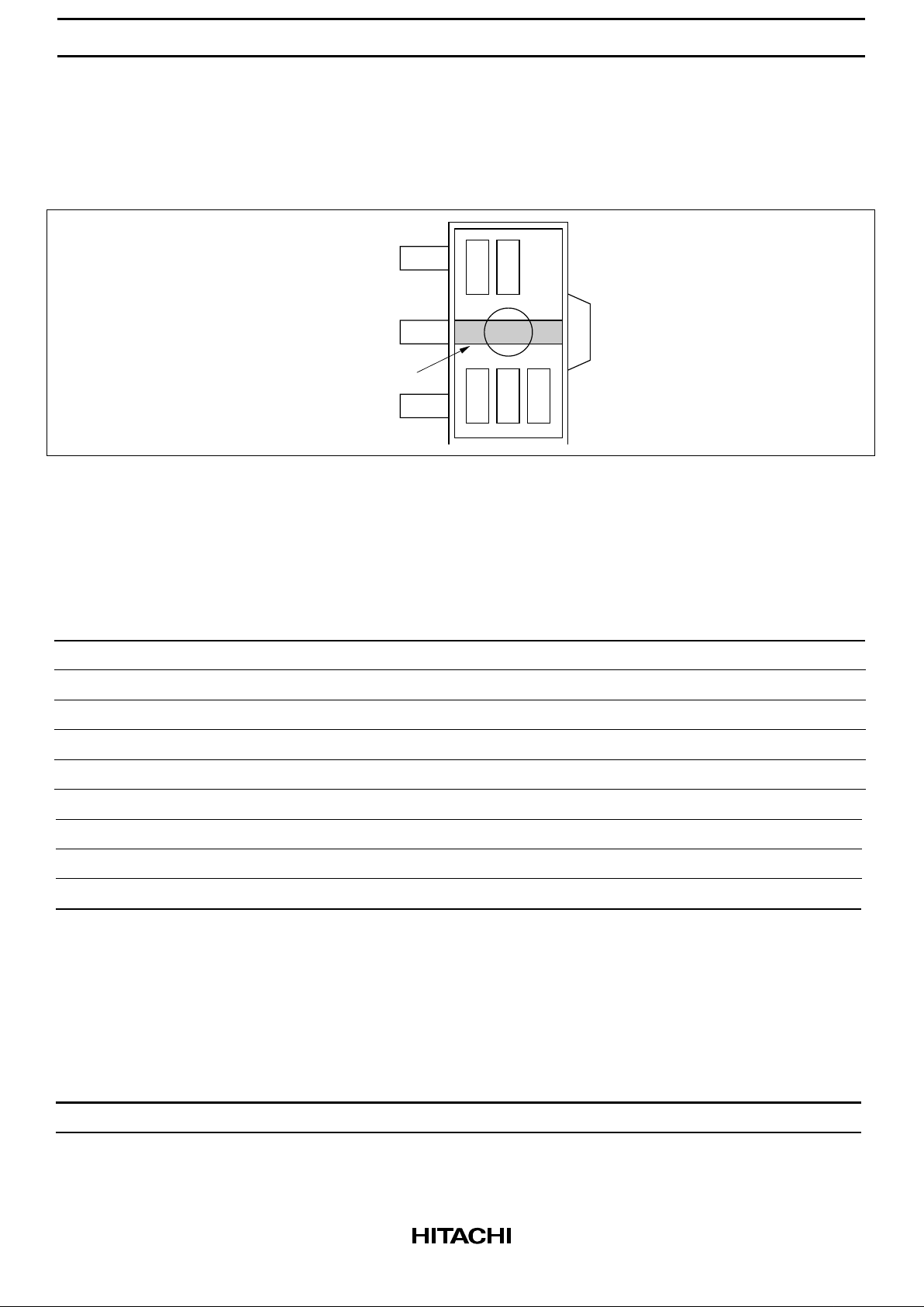
UPAK Product (HA178L00UA) Mark Patterns
The mark patterns shown below are used. on UPAK products, as the package is small. Note that the product
code and mark pattern are different.The pattern is laser-printed.
(1) (2)
(3) (4) (5)
Band Mark
OUT
GND
IN
Notes: 1. Boxes (1) to (5) in the figures show the position of the letters or numerals, and are not actually
marked on the package.
2. (1) and (2) show the product-specific mark pattern. (see table 1)
Table 1
Output Voltage (V) Product No. Mark Pattern (2 digit)
2.5 HA178L02UA 8A
5 HA178L05UA 8B
5.6 HA178L56UA 8C
6 HA178L06UA 8D
8 HA178L08UA 8E
9 HA178L09UA 8F
10 HA178L10UA 8G
12 HA178L12UA 8H
15 HA178L15UA 8J
3. (3) shows the production year code (the last digit of the year).
4. (4) shows the production month code (see table 2).
Table 2
Production Month 1 23456789101112
Marked Code A B C D E F G H J K L M
5. (5) shows the production week code.

HA178L00 Series
5
Absolute Maximum Ratings (Ta = 25°C)
Item Symbol Rating Unit Note
Input voltage V
IN
35 V
Power dissipation P
T
800 mW TO-92M*
1
800 mW UPAK*
2
Operating ambient temperature Topr –20 to +75 °C TO-92M
–20 to +85 °C UPAK
Storage temperature Tstg –55 to +150 °C
Note: 1. Ta ≤ 25°C, If Ta >25°C, derate by 6.4 mW/°C (See figure A)
2. 15mm × 25mm × 0.7 mm alumina ceramic board, Ta ≤ 25°C (See figure B)
1,000
800
600
400
200
0
–20 0 25 50 75 100
480
Ambient Temperature Ta (°C)
Maximum Power Dissipation P
T
(mW)
1,200
1,000
800
600
400
200
0
25 50 12575 150
(1)
Ambient Temperature Ta (°C)
AB
Maximum Power Dissipation P
T
(mW)
100
(2)
(1) Non Board
(2) 15mm × 25mm × 0.7mm
Alumina Ceramic Board

HA178L00 Series
6
HA178L02 Electrical Characteristics
(VIN = 10 V, I
OUT
= 40 mA, 0°C Tj 125°C, CIN = 0.33 µF, C
OUT
= 0.1 µF)
HA178L02P
HA178L02
HA178L02PA
HA178L02A
HA178L02UA
Item Symbol Min Typ Max Min Typ Max Unit Test Conditions
Output voltage V
OUT
2.32 2.48 2.64 2.38 2.48 2.58 V Tj = 25°C
Line regulation δV
OLINE
— 35 125 — 35 95 mV Tj = 25°C 7 V ≤ VIN ≤ 20 V
— 30 100 — 30 75 8 V ≤ VIN ≤ 20 V
Load regulation δV
OLOAD
— 14 — — 14 — mV Tj = 25°C 1.0 mA ≤ I
OUT
≤ 150 mA
— 9.5 50 — 9.5 50 1.0 mA ≤ I
OUT
≤ 100 mA
— 4.5 25 — 4.5 25 1.0 mA ≤ I
OUT
≤ 40 mA
Output voltage V
OUT
2.28 — 2.68 2.35 — 2.61 V 7 V ≤ VIN ≤ 20 V,
1.0 mA ≤ I
OUT
≤ 40 mA
2.28 — 2.68 2.35 — 2.61 VIN = 9 V, 1.0 mA ≤ I
OUT
≤ 70 mA
Quiescent
current
I
Q
— 3.0 6.0 — 3.0 6.0 mA Tj= 25°C
Quiescent δI
Q
— — 1.5 — — 1.5 mA Tj= 25°C 8 V ≤ VIN ≤ 20 V
current change
— — 0.2 — — 0.1 1.0 mA ≤ I
OUT
≤ 40 mA
Ripple rejection
ratio
R
REJ
— 60 — — 60 — dB f = 120 Hz,
8.0 V ≤ V
IN
< 18 V, Tj = 25°C
Temperature
coefficient of
output voltage
δV
OUT
/δTj — +0.2 — — +0.2 — mV/°CI
OUT
= 5 mA

HA178L00 Series
7
HA178L05 Electrical Characteristics
(VIN = 10 V, I
OUT
= 40 mA, 0°C Tj 125°C, CIN = 0.33 µF, C
OUT
= 0.1 µF)
HA178L05P
HA178L05
HA178L05PA
HA178L05A
HA178L05UA
Item Symbol Min Typ Max Min Typ Max Unit Test Conditions
Output voltage V
OUT
4.68 5.0 5.32 4.8 5.0 5.2 V Tj = 25°C
Line regulation δV
OLINE
— 55 200 — 55 150 mV Tj = 25°C 7 V ≤ VIN ≤ 20 V
— 45 150 — 45 100 8 V ≤ VIN ≤ 20 V
Load regulation δV
OLOAD
— 16 — — 16 — mV Tj = 25°C 1.0 mA ≤ I
OUT
≤ 150 mA
— 11 60 — 11 60 1.0 mA ≤ I
OUT
≤ 100 mA
— 5.0 30 — 5.0 30 1.0 mA ≤ I
OUT
≤ 40 mA
Output voltage V
OUT
4.6 — 5.4 4.75 — 5.25 V 7 V ≤ VIN ≤ 20 V,
1.0 mA ≤ I
OUT
≤ 40 mA
4.6 — 5.4 4.75 — 5.25 VIN = 10 V, 1.0 mA ≤ I
OUT
≤ 70 mA
Quiescent
current
I
Q
— 3.0 6.0 — 3.0 6.0 mA Tj = 25°C
Quiescent δI
Q
— — 1.5 — — 1.5 mA Tj = 25°C 8.0 V ≤ VIN ≤ 20 V
current change
— — 0.2 — — 0.1 1.0 mA ≤ I
OUT
≤ 40 mA
Ripple rejection
ratio
R
REJ
— 58 — — 58 — dB f = 120 Hz,
8.0 V ≤ V
IN
< 18 V, Tj = 25°C
Temperature
coefficient of
output voltage
δV
OUT
/δTj — +0.1 — — +0.1 — mV/°CI
OUT
= 5 mA
Dropout voltage V
DROP
— 1.7 — — 1.7 — V Tj = 25°C
 Loading...