

HIT 2SJ553-S Datasheet
2SJ553(L),2SJ553(S)
Silicon P Channel MOS FET
High Speed Power Switching
ADE-208-650B (Z)
3rd. Edition
Jun 1998
Features
• Low on-resistance
R
DS(on)
= 0.028Ω typ.
• Low drive current.
• 4V gate drive devices.
• High speed switching.
Outline
1. Gate
2. Drain
3. Source
4. Drain
1
2
3
4
1
2
3
4
LDPAK
D
G
S
2SJ553(L),2SJ553(S)
2
Absolute Maximum Ratings (Ta = 25°C)
Item Symbol Ratings Unit
Drain to source voltage V
DSS
–60 V
Gate to source voltage V
GSS
±20 V
Drain current I
D
–30 A
Drain peak current I
D(pulse)
Note1
–120 A
Body-drain diode reverse drain current I
DR
–30 A
Avalanche current I
AP
Note3
–30 A
Avalanche energy E
AR
Note3
77 mJ
Channel dissipation Pch
Note2
75 W
Channel temperature Tch 150 °C
Storage temperature Tstg –55 to +150 °C
Note: 1. PW ≤ 10µs, duty cycle ≤ 1 %
2. Value at Tc = 25°C
3. Value at Tch = 25°C, Rg ≥ 50 Ω
Electrical Characteristics (Ta = 25°C)
Item Symbol Min Typ Max Unit Test Conditions
Drain to source breakdown voltage V
(BR)DSS
–60 — — V ID = –10mA, VGS = 0
Gate to source breakdown voltage V
(BR)GSS
±20——V I
G
= ±100µA, VDS = 0
Zero gate voltege drain current I
DSS
— — –10 µAVDS = –60 V, VGS = 0
Gate to source leak current I
GSS
——±10 µAVGS = ±16V, VDS = 0
Gate to source cutoff voltage V
GS(off)
–1.0 — –2.0 V ID = –1mA, VDS = –10V
Static drain to source on state R
DS(on)
— 0.028 0.037 Ω ID = –15A, VGS = –10V
Note4
resistance R
DS(on)
— 0.038 0.055 Ω ID = –15A, VGS = –4V
Note4
Forward transfer admittance |yfs| 1525—S I
D
= –15A, VDS = –10V
Note4
Input capacitance Ciss — 2500 — pF VDS = –10V
Output capacitance Coss — 1300 — pF VGS = 0
Reverse transfer capacitance Crss — 300 — pF f = 1MHz
Turn-on delay time t
d(on)
— 25 — ns VGS = –10V, ID = –15A
Rise time t
r
— 150 — ns RL = 2Ω
Turn-off delay time t
d(off)
— 350 — ns
Fall time t
f
— 220 — ns
Body–drain diode forward voltage V
DF
— –0.95 — V IF = –30A, VGS = 0
Body–drain diode reverse
recovery time
t
rr
— 100 — ns IF = –30A, VGS = 0
diF/ dt =50A/µs
Note: 4. Pulse test
2SJ553(L),2SJ553(S)
3
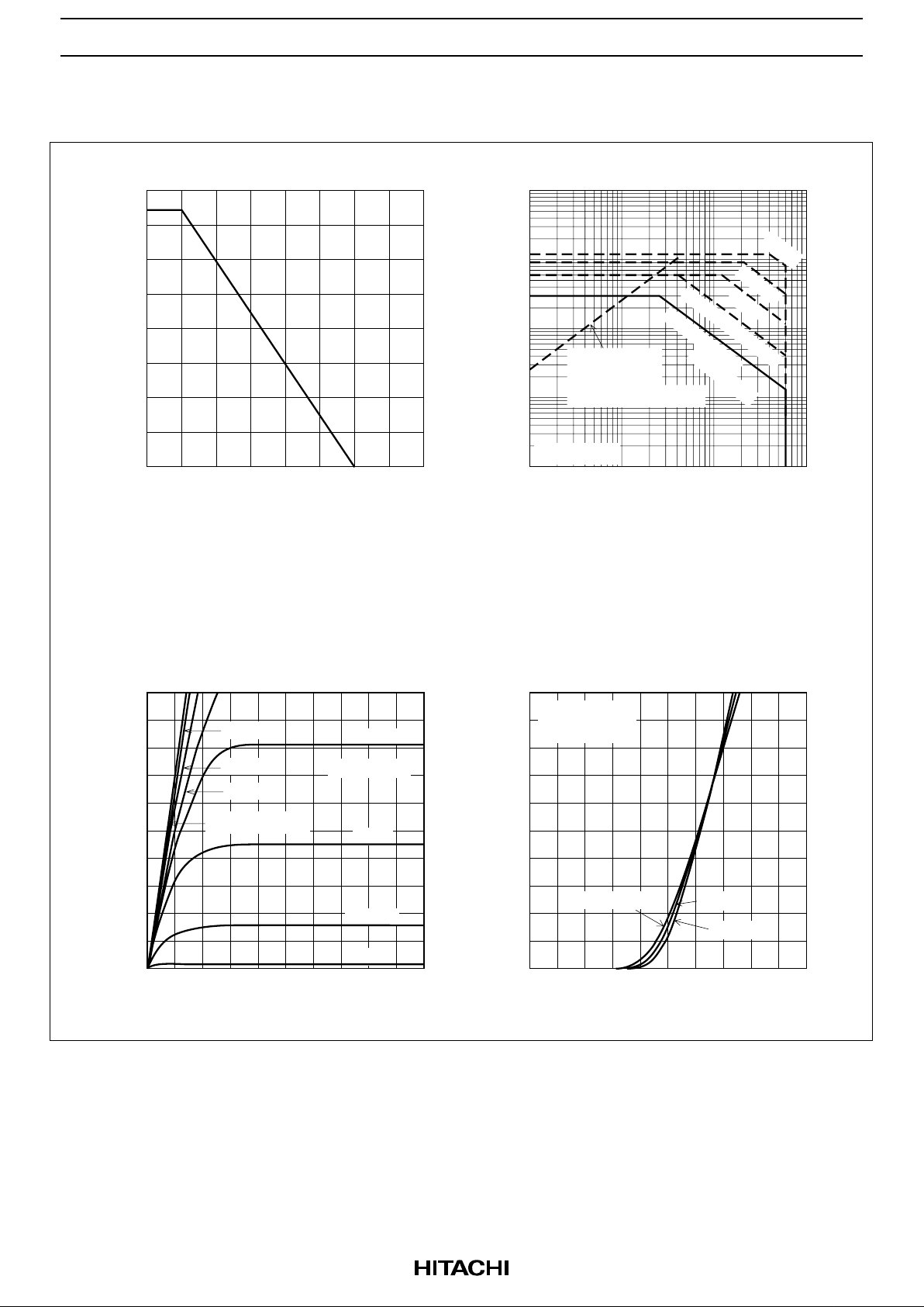
Main Characteristics
80
60
40
20
0
50 100 150 200
–100
–10
–1
–0.1
–0.1 –1 –10
0
–2 –4 –6 –8 –10
0 –1–2–3–4–5
–100
–1000
–50
–40
–30
–20
–10
-25 °C
25 °C
1 ms
Ta = 25 °C
10 µs
DS
PulseTest
V = –10 V
PW = 10 ms (1 shot)
100 µs
–50
–40
–30
–20
–10
–2.5 V
–2 V
V = –10 V
GS
–8 V
–5 V
–3.5 V
–3 V
–4 V
Channel Dissipation Pch (W)
Power vs. Temperature Derating
Drain to Source Voltage V (V)
DS
Drain Current I (A)
D
Maximum Safe Operation Area
Drain to Source Voltage V (V)
DS
Drain Current I (A)
D
Typical Output Characteristics
Gate to Source Voltage V (V)
GS
Typical Transfer Characteristics
Operation in
this area is
limited by R
DS(on)
Drain Current I (A)
D
Case Temperature Tc (°C)
Tc = 75 °C
DC Operation
(Tc = 25 °C)
Pulse Test
 Loading...