

Features
• Low on-resistance
R
= 25 mΩ typ.
DS(on)
• 4V gate drive devices.
• High speed switching
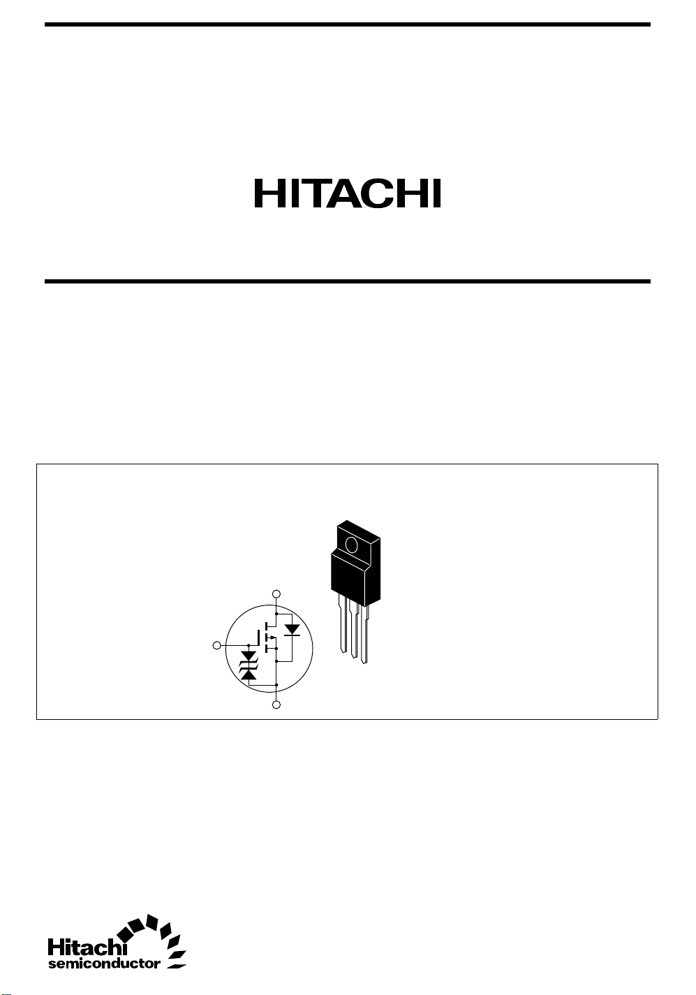
Outline
2SJ471
Silicon P Channel DV–L MOS FET
High Speed Power Switching
ADE-208-540
1st. Edition
TO–220CFM
G
D
1
2
3
S
1. Gate
2. Drain
3. Source

2SJ471
Absolute Maximum Ratings (Ta = 25°C)
Item Symbol Ratings Unit
Drain to source voltage V
Gate to source voltage V
Drain current I
Drain peak current I
Body to drain diode reverse drain current I
Channel dissipation Pch
DSS
GSS
D
D(pulse)
DR
Note1
Note2
Channel temperature Tch 150 °C
Storage temperature Tstg –55 to +150 °C
Notes: 1. PW ≤ 10µs, duty cycle ≤ 1 %
2. Value at Tc = 25°C
–30 V
±20 V
–30 A
–120 A
–30 A
30 W
2

Electrical Characteristics (Ta = 25°C)
Item Symbol Min Typ Max Unit Test Conditions
Drain to source breakdown
V
(BR)DSS
voltage
Gate to source breakdown
V
(BR)GSS
voltage
Zero gate voltege drain
I
DSS
current
Gate to source leak current I
Gate to source cutoff voltage V
Static drain to source on state R
resistance R
GSS
GS(off)
DS(on)
DS(on)
Forward transfer admittance |yfs| 1220—S I
Input capacitance Ciss — 1700 — pF VDS = –10V
Output capacitance Coss — 950 — pF VGS = 0
Reverse transfer capacitance Crss — 260 — pF f = 1MHz
Turn-on delay time t
Rise time t
Turn-off delay time t
Fall time t
Body to drain diode forward
V
d(on)
r
d(off)
f
DF
voltage
Body to drain diode reverse
t
rr
recovery time
Note: 3. Pulse test
–30 — — V ID = –10mA, VGS = 0
±20——V I
— — –10 µAV
——±10 µAV
= ±100µA, VDS = 0
G
= –30 V, VGS = 0
DS
= ±16V, VDS = 0
GS
–1.0 — –2.0 V ID = –1mA, VDS = –10V
—2535mΩI
—4060mΩI
= –15A, VGS = –10V
D
= –15A, VGS = –4V
D
= –15A, VDS = –10V
D
— 20 — ns VGS = –10V, ID = –15A
— 290 — ns RL = 0.67Ω
— 170 — ns
— 130 — ns
— –1.1 — V IF = –30A, VGS = 0
— 70 — ns IF = –30A, VGS = 0
diF/ dt = 50A/µs
2SJ471
Note3
Note3
Note3
3
 Loading...