

2SJ247
Silicon P-Channel MOS FET
Application
High speed power switching
Features
• Low on-resistance
• High speed switching
• Low drive current
• 4 V gate drive device can be driven from 5 V source
• Suitable for switching regulator, DC-DC converter
Outline
TO-220AB
G
1
D
S
2
3
1. Gate
2. Drain
(Flange)
3. Source
2SJ247
Absolute Maximum Ratings (Ta = 25°C)
Item Symbol Ratings Unit
Drain to source voltage V
Gate to source voltage V
Drain current I
Drain peak current I
Body to drain diode reverse drain current I
Channel dissipation Pch*
DSS
GSS
D
D(pulse)
DR
1
*
2
Channel temperature Tch 150 °C
Storage temperature Tstg –55 to +150 °C
Notes: 1. PW ≤ 10 µs, duty cycle ≤ 1%
2. Value at T
= 25°C
C
Electrical Characteristics (Ta = 25°C)
Item Symbol Min Typ Max Unit Test conditions
Drain to source breakdown
V
(BR)DSS
voltage
Gate to source breakdown
V
(BR)GSS
voltage
Gate to source leak current I
Zero gate voltage drain current I
Gate to source cutoff voltage V
Static drain to source on state R
GSS
DSS
GS(off)
DS(on)
resistance — 0.3 0.45 Ω ID = –4 A, VGS = –4 V*
Forward transfer admittance |yfs| 3.0 5.5 — S ID = –4 A, VDS = –10 V*
Input capacitance Ciss — 880 — pF VDS = –10 V, VGS = 0,
Output capacitance Coss — 325 — pF f = 1 MHz
Reverse transfer capacitance Crss — 80 — pF
Turn-on delay time t
Rise time t
Turn-off delay time t
Fall time t
Body to drain diode forward
V
d(on)
r
d(off)
f
DF
voltage
Body to drain diode reverse
t
rr
recovery time
–100 — — V ID = –10 mA, VGS = 0
±20——V I
——±10 µAVGS = ±16 V, VDS = 0
— — –250 µAVDS = –80 V, VGS = 0
–1.0 — –2.0 V ID = –1 mA, VDS = –10 V
— 0.25 0.3 Ω ID = –4 A, VGS = –10 V*
— 12 — ns ID = –4 A, VGS = –10 V,
— 47 — ns RL = 7.5 Ω
— 150 — ns
—75—ns
— –1.0 — V IF = –8 A, VGS = 0
— 170 — ns IF = –8 A, VGS = 0,
–100 V
±20 V
–8 A
–32 A
–8 A
40 W
= ±100 µA, VDS = 0
G
di
/dt = 50 A/µs
F
1
1
1
2
2SJ247
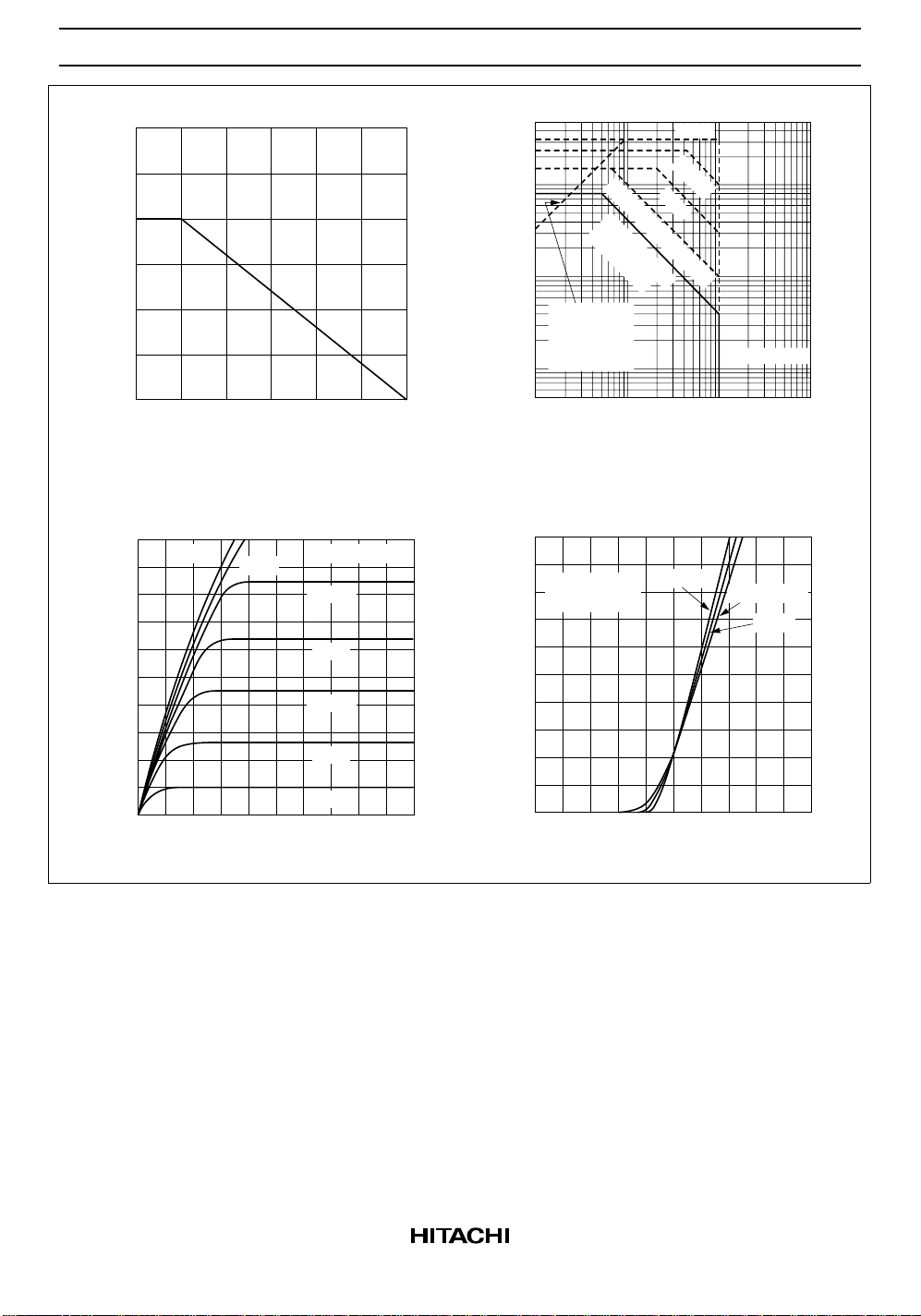
Power vs. Temperature Derating
60
40
20
Channel Dissipation Pch (W)
0 10050 150
Case Temperature Tc (°C)
Typical Output Characteristics
–20
D
–16
–12
–10 V
–6 V
Pulse Test
–4.5 V
–4 V
–50
Maximum Safe Operation Area
–30
PW = 10 ms (1 Shot)
DC Operation
(Tc = 25°C)
D
–10
–3
–1
Operation in
–0.3
–0.1
this area
is limited
by R (on)
DS
Drain Current I (A)
–0.05
–3 –10 –300 –1000
–1 –30 –100
Drain to Source Voltage V (V)
Typical Transfer Characteristics
–10
Pulse Test
–8
V = –10 V
DS
D
–6
10 s
100 s
1 ms
–25°C
µ
µ
Ta = 25°C
DS
Tc = 75°C
25°C
–8
Drain Current I (A)
–4
–3.5 V
–3 V
–2.5 V
0 –4 –8 –12 –16 –20
Drain to Source Voltage V (V)
DS
–4
Drain Current I (A)
–2
0 –2 –4 –6 –8 –10
Gate to Source Voltage V (V)
GS
3
 Loading...