

2SJ186
Silicon P-Channel MOS FET
Application
High speed power switching
Features
• Low on-resistance
• High speed switching
• Low drive current
• Suitable for motor drive, DC-DC converter, power switch and solenoid drive
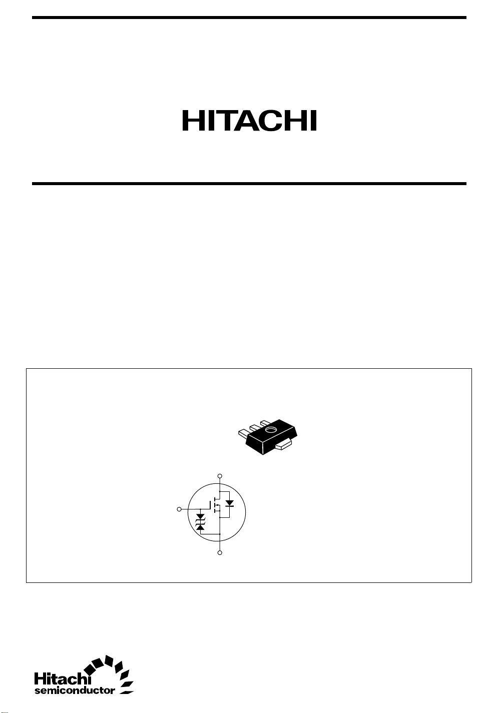
Outline
UPAK
G
1
2
3
4
D
1. Gate
2. Drain
3. Source
4. Drain
S

2SJ186
Absolute Maximum Ratings (Ta = 25°C)
Item Symbol Ratings Unit
Drain to source voltage V
Gate to source voltage V
Drain current I
Drain peak current I
Body to drain diode reverse drain current I
Channel dissipation Pch*
DSS
GSS
D
D(pulse)
DR
1
*
2
Channel temperature Tch 150 °C
Storage temperature Tstg –55 to +150 °C
Notes: 1. PW ≤ 10 µs, duty cycle ≤ 1%
2. When using the alumina ceramic board (12.5×20×0.7 mm)
–200 V
±15 V
–0.5 A
–1.0 A
–0.5 A
1W
2

2SJ186
Electrical Characteristics (Ta = 25°C)
Item Symbol Min Typ Max Unit Test conditions
Drain to source breakdown
V
(BR)DSS
voltage
Gate to source breakdown
V
(BR)GSS
voltage
Gate to source leak current I
Zero gate voltage drain current I
Gate to source cutoff voltage V
Static drain to source on state R
GSS
DSS
GS(off)
DS(on)
resistance — 10.0 15.0 ID = –1 A, VGS = –10 V*
Forward transfer admittance |yfs| 0.18 0.3 — S ID = –0.25 A, VDS = –10 V*
Input capacitance Ciss — 75 — pF VDS = –10 V, VGS = 0,
Output capacitance Coss — 32 — pF f = 1 MHz
Reverse transfer capacitance Crss — 5 — pF
Turn-on delay time t
Rise time t
Turn-off delay time t
Fall time t
Body to drain diode forward
V
d(on)
r
d(off)
f
DF
voltage
Body to drain diode reverse
t
rr
recovery time
Note: 1. Pulse test
–200 — — V ID = –10 mA, VGS = 0
±15——V I
= ±100 µA, VDS = 0
G
——±10 µAVGS = ±12 V, VDS = 0
— — –50 µAVDS = –160 V, VGS = 0
–2.0 — –4.0 V ID = –1 mA, VDS = –10 V
— 8.0 12.0 Ω ID = –0.25 A, VGS = –10 V*
1
—6 —nsI
—6 —nsR
= –0.25 A, VGS = –10 V,
D
= 120 Ω
L
—17—ns
—15—ns
— 0.95 — V IF = –0.5 A, VGS = 0
— 100 — ns IF = –0.5 A, VGS = 0,
di
/dt = 50 A/µs
F
1
1
Marking for 2SJ186 is “CY”.
3
 Loading...